background image

Thermal Management

66

Datasheet, Volume 1

5.3

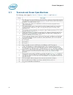
Thermal and Power Specifications

The following notes apply to 

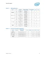
Table 5-1

Table 5-2

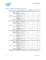
Table 5-3

, and 

Table 5-4

.

Notes

Description

1

The TDPs given are not the maximum power the processor can generate. Analysis indicates that 

real applications are unlikely to cause the processor to consume the theoretical maximum power 

dissipation for sustained periods of time.

2

TDP workload may consist of a combination of a CPU-core intensive and a graphics-core 

intensive applications.

3

The thermal solution needs to ensure that the processor temperature does not exceed the 

maximum junction temperature (Tj,max) limit, as measured by the DTS and the critical 

temperature bit.

4

The processor junction temperature is monitored by Digital Temperature Sensors (DTS). For DTS 

accuracy, refer to 

Section 5.4.1.2.1

.

5

Digital Thermal Sensor (DTS) based fan speed control is required to achieve optimal thermal 

performance. Intel recommends full cooling capability well before the DTS reading reaches 

Tj,Max. An example of this is Tj,Max – 10 ºC.

6

The idle power specifications are not 100% tested. These power specifications are determined 

by the characterization at higher temperatures and extrapolating the values for the junction 

temperature indicated.

7

At Tj of Tj,max

8

At Tj of 50 ºC

9

At Tj of 35 ºC

10

Can be modified at runtime by MSR writes, with MMIO and with PECI commands

11

'Turbo Time Parameter' is a mathematical parameter (unit in seconds) that controls the 

processor turbo algorithm using a moving average of energy usage. Avoid setting the Turbo 

Time Parameter to a value less than 0.1 seconds. Refer to 

Section 5.2.4

 for further information.

12

Shown limit is a time averaged power, based upon the Turbo Time Parameter. Absolute product 

power may exceed the set limits for short durations or under virus or uncharacterized 

workloads.

13

Processor will be controlled to specified power limit as described in 

Section 5.2.1

. If the power 

value and/or ‘Turbo Time Parameter’ is changed during runtime, it may take a short period of 

time (approximately 3 to 5 times the ‘Turbo Time Parameter’) for the algorithm to settle at the 

new control limits.

14

This is a hardware default setting and not a behavioral characteristic of the part.

15

For controllable turbo workloads, the limit may be exceeded for up to 10 ms.

16

Tj

MAX

 may vary between processor SKUs.

Summary of Contents for 2ND GENERATION CORE PROCESSOR FAMILY DESKTOP - VOLUME 1 01-2011

Page 1: ...2 001 2nd Generation Intel Core Processor Family Mobile Datasheet Volume 1 Supporting Intel Core i7 Mobile Extreme Edition Processor Series and Intel Core i5 and i7 Mobile Processor Series This is Volume 1 of 2 January 2011 ...

Page 2: ...our hardware and software configurations Consult with your system vendor for more information No computer system can provide absolute security under all conditions Intel Trusted Execution Technology Intel TXT requires a computer system with Intel Virtualization Technology an Intel TXT enabled processor chipset BIOS Authenticated Code Modules and an Intel TXT compatible measured launched environmen...

Page 3: ...ed 23 2 1 2 System Memory Timing Support 24 2 1 3 System Memory Organization Modes 24 2 1 3 1 Single Channel Mode 24 2 1 3 2 Dual Channel Mode Intel Flex Memory Technology Mode 24 2 1 4 Rules for Populating Memory Slots 25 2 1 5 Technology Enhancements of Intel Fast Memory Access Intel FMA 26 2 1 5 1 Just in Time Command Scheduling 26 2 1 5 2 Command Overlap 26 2 1 5 3 Out of Order Scheduling 26 2...

Page 4: ...y 40 3 4 Intel Turbo Boost Technology 41 3 4 1 Intel Turbo Boost Technology Frequency 41 3 4 2 Intel Turbo Boost Technology Graphics Frequency 42 3 5 Intel Advanced Vector Extensions AVX 42 3 6 Advanced Encryption Standard New Instructions AES NI 42 3 6 1 PCLMULQDQ Instruction 43 3 7 Intel 64 Architecture x2APIC 43 4 Power Management 45 4 1 ACPI States Supported 45 4 1 1 System States 45 4 1 2 Pro...

Page 5: ...agement 63 5 1 Thermal Design Power TDP and Junction Temperature Tj 63 5 2 Thermal Considerations 63 5 2 1 Intel Turbo Boost Technology Power Control and Reporting 64 5 2 2 Package Power Control 65 5 2 3 Power Plane Control 65 5 2 4 Turbo Time Parameter 65 5 3 Thermal and Power Specifications 66 5 4 Thermal Management Features 70 5 4 1 Processor Package Thermal Features 70 5 4 1 1 Adaptive Thermal...

Page 6: ...t SA VCC VID 92 7 5 Reserved or Unused Signals 92 7 6 Signal Groups 93 7 7 Test Access Port TAP Connection 95 7 8 Storage Condition Specifications 95 7 9 DC Specifications 96 7 9 1 Voltage and Current Specifications 97 7 10 Platform Environmental Control Interface PECI DC Specifications 103 7 10 1 PECI Bus Architecture 103 7 10 2 PECI DC Characteristics 104 7 10 3 Input Device Hysteresis 105 8 Pro...

Page 7: ...op View Upper Left Quadrant 123 8 6 BGA1224 Ballmap Top View Upper Right Quadrant 124 8 7 BGA1224 Ballmap Top View Lower Left Quadrant 125 8 8 BGA1224 Ballmap Top View Lower Right Quadrant 126 8 9 BGA1023 Ballmap Top View Upper Left Quadrant 142 8 10 BGA1023 Ballmap Top View Upper Right Quadrant 143 8 11 BGA1023 Ballmap Top View Lower Left Quadrant 144 8 12 BGA1023 Ballmap Top View Lower Right Qua...

Page 8: ... 6 6 PCI Express Graphics Interface Signals 80 6 7 Embedded Display Port Signals 81 6 8 Intel Flexible Display Interface 81 6 9 DMI Processor to PCH Serial Interface 81 6 10 PLL Signals 82 6 11 TAP Signals 82 6 12 Error and Thermal Protection 83 6 13 Power Sequencing 83 6 14 Processor Power Signals 84 6 15 Sense Pins 84 6 16 Ground and NCTF 85 6 17 Future Compatibility 85 6 18 Processor Internal P...

Page 9: ...l Limits 104 8 1 rPGA988B Processor Pin List by Pin Name 112 8 2 BGA1224 Processor Ball List by Ball Name 127 8 3 BGA1023 Processor Ball List by Ball Name 146 9 1 DDR Data Swizzling Table Channel A 170 9 2 DDR Data Swizzling Table Channel B 171 ...

Page 10: ...10 Datasheet Volume 1 Revision History Revision Number Description Date 001 Initial Release January 2011 ...

Page 11: ...cations pinout and signal definitions interface functional descriptions thermal specifications and additional feature information pertinent to the implementation and operation of the processor on its respective platform Note Throughout this document the 2nd Generation Intel Core processor family mobile may be referred to simply as processor Note Throughout this document the Intel Core i7 Extreme E...

Page 12: ... G raphics PEG AnalogC RT G igabit NetworkC onnection USB2 0 Intel HDAudio FWH Super I O Serial ATA DDR3 PC I Express 2 0 1 x16 or 2x8 8 PC I Express 2 0 x1 Ports 5 G T s SPI Digital Display x 3 PC I Express SPI Flashx 2 LPC SMBUS2 0 G PIO LVDSFlat Panel WiFi WiMax C ontroller Link1 EmbeddedDisplay Port Processor PEC I Platform Controller Hub PCH Intel Management Engine ...

Page 13: ...vanced Vector Extensions Intel AVX Advanced Encryption Standard New Instructions AES NI PCLMULQDQ Instruction 1 2 Interfaces 1 2 1 System Memory Support Two channels of DDR3 memory with a maximum of one SO DIMM per channel Single channel and dual channel memory organization modes Data burst length of eight for all memory organization modes Memory DDR3 data transfer rates of 1066 MT s 1333 MT s and...

Page 14: ...the data pins of 2 5 GT s resulting in a real bandwidth per pair of 250 MB s given the 8b 10b encoding used to transmit data across this interface This also does not account for packet overhead and link maintenance Maximum theoretical bandwidth on the interface of 4 GB s in each direction simultaneously for an aggregate of 8 GB s when x16 Gen 1 Gen 2 Raw bit rate on the data pins of 5 0 GT s resul...

Page 15: ...nzero with an Unsupported Request response Upstream write transactions to addresses above 64 GB will be dropped Re issues Configuration cycles that have been previously completed with the Configuration Retry status PCI Express reference clock is 100 MHz differential clock Power Management Event PME functions Dynamic width capability Message Signaled Interrupt MSI and MSI X messages Polarity invers...

Page 16: ... PCH end to end lane reversal across the link Supports Half Swing low power low voltage 1 2 4 Platform Environment Control Interface PECI The PECI is a one wire interface that provides a communication channel between a PECI client the processor and a PECI master The processors support the PECI 3 0 Specification 1 2 5 Processor Graphics The Processor Graphics contains a refresh of the sixth generat...

Page 17: ...ed frequency 2 7 GT s data rate Two sideband signals for Display synchronization FDI_FSYNC and FDI_LSYNC Frame and Line Synchronization One Interrupt signal used for various interrupts from the PCH FDI_INT signal shared by both Intel FDI Links PCH supports end to end lane reversal across both links Common 100 MHz reference clock 1 3 Power Management Support 1 3 1 Processor Core Full support of ACP...

Page 18: ...p Throttling Memory Thermal Throttling External Thermal Sensor TS on DIMM and TS on Board Render Thermal Throttling Fan speed control with DTS 1 5 Package The processor is available on two packages A 37 5 x 37 5 mm rPGA package rPGA988B A 31 x 24 mm BGA package BGA1023 or BGA1224 1 6 Terminology Term Description BLT Block Level Transfer CRT Cathode Ray Tube DDR3 Third generation Double Data Rate S...

Page 19: ...ion NCTF locations are typically redundant ground or non critical reserved so the loss of the solder joint continuity at end of life conditions will not affect the overall product functionality PCH Platform Controller Hub The new 2009 chipset with centralized platform capabilities including the main I O interfaces along with display connectivity audio features power management manageability securi...

Page 20: ...Agent memory controller DMI PCIe controllers and display engine power supply VDDQ DDR3 power supply VLD Variable Length Decoding VSS Processor ground x1 Refers to a Link or Port with one Physical Lane x16 Refers to a Link or Port with sixteen Physical Lanes x4 Refers to a Link or Port with four Physical Lanes x8 Refers to a Link or Port with eight Physical Lanes Term Description ...

Page 21: ...hanical Specifications and Design Guidelines www intel com Assets PDF desig nguide 324647 pdf Advanced Configuration and Power Interface Specification 3 0 http www acpi info PCI Local Bus Specification 3 0 http www pcisig com specifica tions PCI Express Base Specification 2 0 http www pcisig com DDR3 SDRAM Specification http www jedec org DisplayPort Specification http www vesa org Intel 64 and IA...

Page 22: ...Introduction 22 Datasheet Volume 1 ...

Page 23: ...hnologies and addressing are supported for x16 and x8 devices There is no support for memory modules with different technologies or capacities on opposite sides of the same memory module If one side of a memory module is populated the other side is either identical or empty Notes 1 System memory configurations are based on availability and are subject to change 2 Interface does not support ULV LV ...

Page 24: ...directed to a single channel Single channel mode is used when either Channel A or Channel B DIMM connectors are populated in any order but not both 2 1 3 2 Dual Channel Mode Intel Flex Memory Technology Mode The IMC supports Intel Flex Memory Technology Mode Memory is divided into a symmetric and an asymmetric zone The symmetric zone starts at the lowest address in each channel and is contiguous u...

Page 25: ... and the single channel zone is the top of memory IMC operates completely in Dual Channel Symmetric mode Note The DRAM device technology and width may vary from one channel to the other 2 1 4 Rules for Populating Memory Slots In all modes the frequency of system memory is the lowest frequency of all memory modules placed in the system as determined through the SPD registers on the memory modules T...

Page 26: ...otocol 2 1 5 3 Out of Order Scheduling While leveraging the Just in Time Scheduling and Command Overlap enhancements the IMC continuously monitors pending requests to system memory for the best use of bandwidth and reduction of latency If there are multiple requests to the same open page these requests would be launched in a back to back manner to make optimum use of the open memory page This abil...

Page 27: ... 8b 10b encoding is used accounts for the 250 MB s where quick calculations would imply 300 MB s The external graphics ports support Gen2 speed as well At 5 0 GT s Gen 2 operation results in twice as much bandwidth per lane as compared to Gen 1 operation When operating with two PCIe controllers each controller can be operating at either 2 5 GT s or 5 0 GT s The PCI Express architecture is specifie...

Page 28: ...calculates and applies data protection code and TLP sequence number and submits them to Physical Layer for transmission across the Link The receiving Data Link Layer is responsible for checking the integrity of received TLPs and for submitting them to the Transaction Layer for further processing On detection of TLP error s this layer is responsible for requesting retransmission of TLPs until infor...

Page 29: ...guration Mechanism section The PCI Express Host Bridge is required to translate the memory mapped PCI Express configuration space accesses from the host processor to PCI Express configuration cycles To maintain compatibility with PCI configuration addressing mechanisms it is recommended that system software access the enhanced configuration space using 32 bit operations 32 bit aligned only See the...

Page 30: ... generate SERR in response to errors never SCI SMI MSI PCI INT or GPE Any DMI related SERR activity is associated with Device 0 2 3 2 Processor PCH Compatibility Assumptions The processor is compatible with the I ntel 6 Series Chipset PCH The processor is not compatible with any previous PCH products Figure 2 5 PCIe Typical Operation 16 lanes Mapping 0 1 2 3 4 5 6 7 8 9 10 11 12 13 14 15 1 X 16 Co...

Page 31: ...ormal No completions from downstream non posted transactions are returned upstream over the DMI link after a link down event 2 4 Processor Graphics Controller GT New Graphics Engine Architecture includes 3D compute elements Multi format hardware assisted decode encode Pipeline and Mid Level Cache MLC for superior high definition playback video quality and improved 3D performance and Media Display ...

Page 32: ...t vertex reference received from the VF unit in the order received 2 4 1 2 3 Geometry Shader GS Stage The GS stage receives inputs from the VS stage Compiled application provided GS programs specifying an algorithm to convert the vertices of an input object into some output primitives For example a GS shader may convert lines of a line strip into polygons representing a corresponding segment of a ...

Page 33: ...e 128 bit BLT engine provides hardware acceleration of block transfers of pixel data for many common Windows operations The BLT engine can be used for the following Move rectangular blocks of data between memory locations Data alignment To perform logical operations raster ops The rectangular block of data does not change as it is transferred between memory locations The allowable memory transfers...

Page 34: ... is clocked by the Core Display Clock 2 4 2 1 1 Planes A and B Planes A and B are the main display planes and are associated with Pipes A and B respectively The two display pipes are independent allowing for support of two independent display streams They are both double buffered which minimizes latency and improves visual quality 2 4 2 1 2 Sprite A and B Sprite A and Sprite B are planes optimized...

Page 35: ...2 4 Embedded DisplayPort eDP The Processor Graphics supports the Embedded Display Port eDP interface intended for display devices that are integrated into the system such as laptop LCD panel The DisplayPort abbreviated DP is different than the generic term display port The DisplayPort specification is a VESA standard DisplayPort consolidates internal and external connection methods to reduce devic...

Page 36: ... the 2x8 PEG is not supported 2 5 Platform Environment Control Interface PECI The PECI is a one wire interface that provides a communication channel between a PECI client processor and a PECI master The processor implements a PECI interface to Allow communication of processor thermal and other information to the PECI master Read averaged Digital Thermal Sensor DTS values for fan speed control 2 6 ...

Page 37: ...performance and robustness Intel VT x specifications and functional descriptions are included in the Intel 64 and IA 32 Architectures Software Developer s Manual Volume 3B and is available at http www intel com products processor manuals index htm The Intel VT d specification and other VT documents can be referenced at http www intel com technology virtualization index htm 3 1 1 Intel VT x Objecti...

Page 38: ...Descriptor table exiting allows a VMM to protect a guest OS from internal malicious software based attack by preventing relocation of key system data structures like IDT interrupt descriptor table GDT global descriptor table LDT local descriptor table and TSS task segment selector A VMM using this feature can intercept by a VM exit attempts to relocate these data structures and prevent them from b...

Page 39: ...ive IOTLB invalidation MSI cycles MemWr to address FEEx_xxxxh not translated Translation faults result in cycle forwarding to VBIOS region byte enables masked for writes Returned data may be bogus for internal agents PEG DMI interfaces return unsupported request status Interrupt Remapping is supported Queued invalidation is supported VT d translation bypass address range is supported Pass Through ...

Page 40: ...om potential corruption The enhanced platform provides these launch and control interfaces using Safer Mode Extensions SMX The SMX interface includes the following functions Measured Verified launch of the MLE Mechanisms to ensure the above measurement is protected and stored in a secure location Protection mechanisms that allow the MLE to control attempts to modify itself For more information ref...

Page 41: ...outside of the processor control the maximum performance cannot be ensured Turbo Mode availability is independent of the number of active cores however the Turbo Mode frequency is dynamic and dependent on the instantaneous application power load the number of active cores user configurable settings operating environment and system design 3 4 1 Intel Turbo Boost Technology Frequency The processor s...

Page 42: ...ng SIMD Extensions SSE from 128 bit vectors into 256 bit vectors Intel AVX addresses the continued need for vector floating point performance in mainstream scientific and engineering numerical applications visual processing recognition data mining synthesis gaming physics cryptography and other areas of applications The enhancement in Intel AVX allows for improved performance due to wider vectors ...

Page 43: ...tination mode interrupt delivery on link based architectures The key enhancements provided by the x2APIC architecture over xAPIC are the following Support for two modes of operation to provide backward compatibility and extensibility for future platform innovations In xAPIC compatibility mode APIC registers are accessed through a memory mapped interface to a 4 KB page identical to the xAPIC archit...

Page 44: ...ics for using the Interrupt Command Register ICR and End Of Interrupt EOI registers have been modified to allow for more efficient delivery and dispatching of interrupts The x2APIC extensions are made available to system software by enabling the local x2APIC unit in the x2APIC mode To benefit from x2APIC capabilities a new Operating System and a new BIOS are both needed with special support for th...

Page 45: ...cessor G1 S4 Suspend to Disk STD All power lost except wakeup on PCH G2 S5 Soft off All power lost except wakeup on PCH Total reboot G3 Mechanical off All power AC and battery removed from system Table 4 2 Processor Core Package State Support State Description C0 Active mode processor executing code C1 AutoHALT state C1E AutoHALT state with lowest frequency and voltage operating point C3 Execution...

Page 46: ...asserted using device self refresh Table 4 4 PCIe Link States State Description L0 Full on Active transfer state L0s First Active Power Management low power state Low exit latency L1 Lowest Active Power Management Longer exit latency L3 Lowest power state power off Longest exit latency Table 4 5 DMI States State Description L0 Full on Active transfer state L0s First Active Power Management low pow...

Page 47: ...Deep Power down G1 S3 Power off Off except RTC Suspend to RAM G1 S4 Power off Off except RTC Suspend to Disk G2 S5 Power off Off except RTC Soft Off G3 NA Power off Power off Hard off Table 4 8 D S and C State Combination Graphics Adapter D State Sleep S State Package C State Description D0 S0 C0 Full On Displaying D0 S0 C1 C1E Auto Halt Displaying D0 S0 C3 Deep sleep Displaying D0 S0 C6 C7 Deep P...

Page 48: ...lished the PLL locks on to the target frequency If the target frequency is lower than the current frequency the PLL locks to the target frequency then transitions to a lower voltage by signaling the target voltage on SVID bus All active processor cores share the same frequency and voltage In a multi core processor the highest frequency P state requested amongst all active cores is selected Softwar...

Page 49: ...omatically resolved by the processor For thread and core C states a transition to and from C0 is required before entering any other C state Figure 4 1 Idle Power Management Breakdown of the Processor Cores Processor Package State Core 1 State Thread 1 Thread 0 Core 0 State Thread 1 Thread 0 Figure 4 2 Thread and Core C State Entry and Exit C1 C1E C7 C6 C3 C0 MWAIT C1 HLT C0 MWAIT C 7 P_LVL4 I ORea...

Page 50: ...re using the P_LVLx I O read interface Each P LVLx is mapped to the supported MWAIT Cx instruction as shown in Table 4 10 The BIOS can write to the C state range field of the PMG_IO_CAPTURE MSR to restrict the range of I O addresses that are trapped and emulate MWAIT like functionality Any P_LVLx reads outside of this range does not cause an I O redirection to MWAIT Cx like request They fall throu...

Page 51: ...mation on C1E see Package C1 C1E 4 2 4 3 Core C3 State Individual threads of a core can enter the C3 state by initiating a P_LVL2 I O read to the P_BLK or an MWAIT C3 instruction A core in C3 state flushes the contents of its L1 instruction cache L1 data cache and L2 cache to the shared L3 cache while maintaining its architectural state All core clocks are stopped at this point Because the core s ...

Page 52: ... summary of the general rules for package C state entry These apply to all package C states unless specified otherwise A package C state request is determined by the lowest numerical core C state amongst all cores A package C state is automatically resolved by the processor depending on the core idle power states and the status of the platform components Each core can be at a lower idle power stat...

Page 53: ...he processor remains in the normal state when at least one of its cores is in the C0 or C1 state or when the platform has not granted permission to the processor to go into a low power state Individual cores may be in lower power idle states while the package is in C0 Table 4 11 Coordination of Core Power States at the Package Level Package C State Core 1 C0 C1 C3 C6 C7 Core 0 C0 C0 C0 C0 C0 C0 C1...

Page 54: ...to the system occurs upon entry to C1 C1E 4 2 5 3 Package C3 State A processor enters the package C3 low power state when At least one core is in the C3 state The other cores are in a C3 or lower power state and the processor has been granted permission by the platform The platform has not granted a request to a package C6 C7 state but has allowed a package C6 state In package C3 state the L3 shar...

Page 55: ...uced by N ways until it is completely flushed The number of ways N is dynamically chosen per concurrent C7 entry Similarly upon exit the L3 cache is gradually expanded based on internal heuristics 4 3 IMC Power Management The main memory is power managed during normal operation and in low power ACPI Cx states 4 3 1 Disabling Unused System Memory Outputs Any system memory SM interface signal that g...

Page 56: ...es Power consumption is defined by IDD2P1 Exiting this mode is defined by tXP but also tXPDLL 10 20 according to DDR type cycles until first data transfer is allowed The processor supports 5 different types of power down The different modes are the power down modes supported by DDR3 and combinations of these The type of CKE power down is defined by the configuration The are options are 1 No power ...

Page 57: ...e idle timer Another option associated with CKE power down is the S_DLL off When this option is enabled the SBR I O slave DLLs go off when all channel ranks are in power down Do not confuse it with the DLL off mode in which the DDR DLLs are off This mode requires to define the I O slave DLL wakeup time 4 3 2 1 Initialization Role of CKE During power up CKE is the only input to the SDRAM that has i...

Page 58: ...uch as CS CKE and ODT for unpopulated SO DIMM slots The I O buffer for an unused signal should be tri stated output driver disabled the input receiver differential sense amp should be disabled and any DLL circuitry related ONLY to unused signals should be disabled The input path must be gated to prevent spurious results due to noise on the unused signals typically handled automatically when input ...

Page 59: ...aphics Dynamic Frequency also known as Turbo Boost Technology is supported and enabled the functionality of Intel GPMT will be maintained by Intel Graphics Dynamic Frequency also known as Turbo Boost Technology 4 6 3 Graphics Render C State Render C State RC6 is a technique designed to optimize the average power to the graphics render engine during times of idleness of the render engine Render C s...

Page 60: ...original input image produced by the operating system or application is analyzed by the Intel DPST subsystem An interrupt to Intel DPST software is generated whenever a meaningful change in the image attributes is detected A meaningful change is when the Intel DPST software algorithm determines that enough brightness contrast or color change has occurred to the displaying images that the image enh...

Page 61: ...ftware will automatically switch to a lower refresh rate for maximum battery life when the notebook is on battery power and when the user has selected enabled this feature There are two distinct implementations of Intel DRRS static and seamless The static Intel DRRS method uses a mode change to assign the new refresh rate The seamless Intel DRRS method is able to accomplish the refresh rate assign...

Page 62: ...Power Management 62 Datasheet Volume 1 ...

Page 63: ...tel Turbo Boost Technology applications are expected to run closer to TDP more often as the processor attempts to take advantage of available headroom in the platform to maximize performance The processor may also exceed the TDP for short durations after a period of lower power operation due to its turbo feature This feature is intended to take advantage of available thermal capacitance in the the...

Page 64: ...m will use this parameter to maintain time averaged power at or below POWER_LIMIT_1 The default value is 1 second however 28 seconds is recommended for most mobile applications POWER_LIMIT_2 TURBO_POWER_LIMIT MSR 610h bits 46 32 This value establishes the upper power limit of turbo operation above TDP primarily for platform power supply considerations Power may exceed this limit for up to 10 mS Th...

Page 65: ...unction is similar to the package level long duration window control 5 2 4 Turbo Time Parameter Turbo Time Parameter is a mathematical parameter units in seconds that controls the processor turbo algorithm using an exponentially weighted moving average of energy usage During a maximum power turbo event of about 1 25 x TDP the processor could sustain Power_Limit_2 for up to approximately 1 5 the Tu...

Page 66: ...cations are not 100 tested These power specifications are determined by the characterization at higher temperatures and extrapolating the values for the junction temperature indicated 7 At Tj of Tj max 8 At Tj of 50 ºC 9 At Tj of 35 ºC 10 Can be modified at runtime by MSR writes with MMIO and with PECI commands 11 Turbo Time Parameter is a mathematical parameter unit in seconds that controls the p...

Page 67: ...0 MHz 650 MHz up to 1300 MHz 26 Low Voltage HFM 2 1 GHz up to 3 2 GHz 500 MHz up to 1100 MHz 25 W 1 2 7 LFM 800 MHz 500 MHz up to 1100 MHz 12 Ultra Low Voltage HFM 1 4 GHz up to 2 7 GHz 350 MHz up to 1000 MHz 17 W 1 2 7 LFM 800 MHz 350 MHz up to 1000 MHz 10 Table 5 2 Junction Temperature Specification Segment Symbol Package Turbo Parameter Min Default Max Units Notes Extreme Edition XE TJ Junction...

Page 68: ...OWER_LIMIT MSR 0610h bits 14 0 40 45 48 W 10 12 13 14 Short P package Short duration turbo power limit POWER_LIMIT_2 in TURBO_POWER_LIMIT MSR 0610h bits 46 32 40 1 25 x 45 60 W 10 14 15 Dual Core SV Turbo Time Parameter package Processor turbo long duration time window POWER_LIMIT_1_TIME in TURBO_POWER_LIMIT MSR 0610h bits 23 17 0 001 1 64 S 10 11 14 Long P package Long duration turbo power limit ...

Page 69: ...in the Package C6 state 4 W 6 9 PC7 Idle power in the Package C7state 3 85 W 6 9 Quad Core SV PC1E Idle power in the Package C1e state 11 W 6 8 PC6 Idle power in the Package C6 state 3 9 W 6 9 PC7 Idle power in the Package C7state 3 8 W 6 9 Dual Core SV PC1E Idle power in the Package C1e state 8 8 W 6 8 PC6 Idle power in the Package C6 state 3 1 W 6 9 PC7 Idle power in the Package C7state 2 95 W 6...

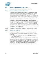
Page 70: ...uses both the processor core and graphics core to reduce frequency and voltage adaptively The TCC will remain active as long as any package temperature exceeds its specified limit Therefore the Adaptive Thermal Monitor will continue to reduce the package frequency and voltage until the TCC is de activated Caution The Adaptive Thermal Monitor must be enabled for the processor to remain within speci...

Page 71: ... are reduced while minimizing performance degradation A small amount of hysteresis has been included to prevent an excessive amount of operating point transitions when the processor temperature is near its maximum operating temperature Once the temperature has dropped below the maximum operating temperature and the hysteresis timer has expired the operating frequency and voltage transition back to...

Page 72: ...clock on time and total time specific to the processor The duty cycle is factory configured to 25 on and 75 off and cannot be modified The period of the duty cycle is configured to 32 microseconds when the TCC is active Cycle times are independent of processor frequency A small amount of hysteresis has been included to prevent excessive clock modulation when the processor temperature is near its m...

Page 73: ...lative offset from Tj max The DTS does not report temperatures greater than Tj max The DTS relative temperature readout directly impacts the Adaptive Thermal Monitor trigger point When a package DTS indicates that it has reached the TCC activation a reading of 0h except when the TCC activation offset is changed the TCC will activate and indicate a Adaptive Thermal Monitor event A TCC activation wi...

Page 74: ... will cool down as a result of reduced processor power consumption Bi directional PROCHOT can allow VR thermal designs to target thermal design current ICCTDC instead of maximum current Systems should still provide proper cooling for the VR and rely on bi directional PROCHOT only as a backup in case of system cooling failure Overall the system thermal design should allow the power delivery circuit...

Page 75: ...ure remains high a critical temperature status and sticky bit are latched in the PACKAGE_THERM_STATUS MSR 1B1h and also generates a thermal interrupt if enabled For more details on the interrupt mechanism refer to the Intel 64 and IA 32 Architectures Software Developer s Manuals 5 4 2 Processor Core Specific Thermal Features 5 4 2 1 On Demand Mode The processor provides an auxiliary mechanism that...

Page 76: ...ronment Control Interface PECI is a one wire interface that provides a communication channel between Intel processor and chipset components to external monitoring devices The processor implements a PECI interface to allow communication of processor thermal information to other devices on the platform The processor provides a digital thermal sensor DTS for fan speed control The DTS is calibrated at...

Page 77: ... coupled The buffers are not 3 3 V tolerant Refer to the PCIe specification eDP Embedded Display Port interface signals These signals are compatible with VESA Revision 1 0 DP specifications and the interface is AC coupled The buffers are not 3 3 V tolerant FDI Intel Flexible Display interface signals These signals are based on PCI Express 2 0 Signaling Environment AC Specifications 2 7 GT s but ar...

Page 78: ...d and write transactions I O DDR3 SA_DQ 63 0 Data Bus Channel A data signal interface to the SDRAM data bus I O DDR3 SA_MA 15 0 Memory Address These signals are used to provide the multiplexed row and column address to the SDRAM O DDR3 SA_CK 1 0 SDRAM Differential Clock Channel A SDRAM Differential clock signal pair The crossing of the positive edge of SA_CK and the negative edge of its complement...

Page 79: ...5 0 Memory Address These signals are used to provide the multiplexed row and column address to the SDRAM O DDR3 SB_CK 1 0 SDRAM Differential Clock Channel B SDRAM Differential clock signal pair The crossing of the positive edge of SB_CK and the negative edge of its complement SB_CK are used to sample the command and control signals on the SDRAM O DDR3 SB_CK 1 0 SDRAM Inverted Differential Clock Ch...

Page 80: ...for these lands I CMOS PM_SYNC Power Management Sync A sideband signal to communicate power management status from the platform to the processor I CMOS RESET Platform Reset pin driven by the PCH I CMOS RSVD RSVD_TP RSVD_NCTF RESERVED All signals that are RSVD and RSVD_NCTF must be left unconnected on the board However Intel recommends that all RSVD_TP signals have using test points No Connect Test...

Page 81: ...X 3 0 FDI0_TX 3 0 Intel Flexible Display Interface Transmit Differential Pair Pipe A O FDI FDI0_FSYNC 0 Intel Flexible Display Interface Frame Sync Pipe A I CMOS FDI0_LSYNC 0 Intel Flexible Display Interface Line Sync Pipe A I CMOS FDI1_TX 3 0 FD1I_TX 3 0 Intel Flexible Display Interface Transmit Differential Pair Pipe B O FDI FDI1_FSYNC 1 Intel Flexible Display Interface Frame Sync Pipe B I CMOS ...

Page 82: ...debug port interposer so that an in target probe can drive system reset O PRDY PRDY is a processor output used by debug tools to determine processor debug readiness O Asynchronous CMOS PREQ PREQ is used by debug tools to request debug operation of the processor I Asynchronous CMOS TCK TCK Test Clock This signal provides the clock input for the processor Test Bus also known as the Test Access Port ...

Page 83: ... processor protects itself from catastrophic overheating by use of an internal thermal sensor This sensor is set well above the normal operating temperature to ensure that there are no false trips The processor will stop all execution when the junction temperature exceeds approximately 130 C This is signaled to the system by the THERMTRIP pin O Asynchronous CMOS Table 6 13 Power Sequencing Signal ...

Page 84: ...ption Direction Buffer Type VCC_SENSE VSS_SENSE VCC_SENSE and VSS_SENSE provide an isolated low impedance connection to the processor core voltage and ground They can be used to sense or measure voltage near the silicon O Analog VAXG_SENSE VSSAXG_SENSE VAXG_SENSE and VSSAXG_SENSE provide an isolated low impedance connection to the VAXG voltage and ground They can be used to sense or measure voltag...

Page 85: ...PLL is required if connected to the DF_TVS strap on the PCH SA_DIMM_VREFDQ SB_DIMM_VREFDQ Memory Channel A B DIMM DQ Voltage Reference These signals are not used by the processors and are for future compatibility only No connection is required VCCIO_SEL Voltage selection for VCCIO This pin must be pulled high on the motherboard when using dual rail voltage regulator which will be used for future c...

Page 86: ...Signal Description 86 Datasheet Volume 1 ...

Page 87: ...large number of transistors and high internal clock speeds the processor is capable of generating large current swings between low and full power states To keep voltages within specification output decoupling must be properly designed Caution Design the board to ensure that the voltage provided to the processor remains within the specifications listed in Table 7 3 Failure to do so can result in ti...

Page 88: ...r to minimize the power of the part A voltage range is provided in Table 7 1 The specifications are set so that one voltage regulator can operate with all supported frequencies Individual processor VID values may be set during manufacturing so that two devices at the same core frequency may have different default VID settings This is shown in the VID range values in Table 7 5 The processor provide...

Page 89: ...1 0 0 0 1 1 1 0 33000 1 0 0 1 0 0 0 1 9 1 0 97000 0 0 0 1 0 0 1 0 1 2 0 33500 1 0 0 1 0 0 1 0 9 2 0 97500 0 0 0 1 0 0 1 1 1 3 0 34000 1 0 0 1 0 0 1 1 9 3 0 98000 0 0 0 1 0 1 0 0 1 4 0 34500 1 0 0 1 0 1 0 0 9 4 0 98500 0 0 0 1 0 1 0 1 1 5 0 35000 1 0 0 1 0 1 0 1 9 5 0 99000 0 0 0 1 0 1 1 0 1 6 0 35500 1 0 0 1 0 1 1 0 9 6 0 99500 0 0 0 1 0 1 1 1 1 7 0 36000 1 0 0 1 0 1 1 1 9 7 1 00000 0 0 0 1 1 0 0 ...

Page 90: ...19500 0 0 1 1 1 1 1 1 3 F 0 56000 1 0 1 1 1 1 1 1 B F 1 20000 0 1 0 0 0 0 0 0 4 0 0 56500 1 1 0 0 0 0 0 0 C 0 1 20500 0 1 0 0 0 0 0 1 4 1 0 57000 1 1 0 0 0 0 0 1 C 1 1 21000 0 1 0 0 0 0 1 0 4 2 0 57500 1 1 0 0 0 0 1 0 C 2 1 21500 0 1 0 0 0 0 1 1 4 3 0 58000 1 1 0 0 0 0 1 1 C 3 1 22000 0 1 0 0 0 1 0 0 4 4 0 58500 1 1 0 0 0 1 0 0 C 4 1 22500 0 1 0 0 0 1 0 1 4 5 0 59000 1 1 0 0 0 1 0 1 C 5 1 23000 0 ...

Page 91: ...41000 0 1 1 0 1 0 1 0 6 A 0 77500 1 1 1 0 1 0 1 0 E A 1 41500 0 1 1 0 1 0 1 1 6 B 0 78000 1 1 1 0 1 0 1 1 E B 1 42000 0 1 1 0 1 1 0 0 6 C 0 78500 1 1 1 0 1 1 0 0 E C 1 42500 0 1 1 0 1 1 0 1 6 D 0 79000 1 1 1 0 1 1 0 1 E D 1 43000 0 1 1 0 1 1 1 0 6 E 0 79500 1 1 1 0 1 1 1 0 E E 1 43500 0 1 1 0 1 1 1 1 6 F 0 80000 1 1 1 0 1 1 1 1 E F 1 44000 0 1 1 1 0 0 0 0 7 0 0 80500 1 1 1 1 0 0 0 0 F 0 1 44500 0 ...

Page 92: ... Arbitrary connection of these signals to VCC VCCIO VDDQ VCCPLL VCCSA VAXG VSS or to any other signal including each other may result in component malfunction or incompatibility with future processors See Chapter 8 for a pin listing of the processor and the location of all reserved signals For reliable operation always connect unused inputs or bi directional signals to an appropriate signal level ...

Page 93: ... SA_CK 1 0 SB_CK 1 0 SB_CK 1 0 DDR3 Command Signals2 Single Ended DDR3 Output SA_BS 2 0 SB_BS 2 0 SA_WE SB_WE SA_RAS SB_RAS SA_CAS SB_CAS SA_MA 15 0 SB_MA 15 0 DDR3 Control Signals2 Single Ended DDR3 Output SA_CKE 1 0 SB_CKE 1 0 SA_CS 1 0 SB_CS 1 0 SA_ODT 1 0 SB_ODT 1 0 SM_DRAMRST DDR3 Data Signals2 Single ended DDR3 Bi directional SA_DQ 63 0 SB_DQ 63 0 Differential DDR3 Bi directional SA_DQS 7 0 ...

Page 94: ...S_VAL_SENSE VAXG_VAL_SENSE VSSAXG_VAL_SENSE Power Ground Other Single Ended Power VCC VCCIO VCCSA VCCPLL VDDQ VAXG VCCPQE 3 VCCDQ 3 Ground VSS VSS_NCTF 3 DC_TEST_xx No Connect RSVD RSVD_NCTF Test Point RSVD_TP Other SKTOCC PROC_DETECT 3 PCI Express Graphics Differential PCI Express Input PEG_RX 15 0 PEG_RX 15 0 Differential PCI Express Output PEG_TX 15 0 PEG_TX 15 0 Single Ended Analog Input PEG_I...

Page 95: ...rocessor supports Boundary Scan JTAG IEEE 1149 1 2001 and IEEE 1149 6 2003 standards Note that some small portion of the I O pins may support only one of these standards 7 8 Storage Condition Specifications Environmental storage condition limits define the temperature and relative humidity that the device is exposed to while being stored in a moisture barrier bag The specified storage conditions a...

Page 96: ...raints imposed by Tsustained storage and customer shelf life in applicable Intel boxes and bags 7 9 DC Specifications The processor DC specifications in this section are defined at the processor pins unless noted otherwise See Chapter 8 for the processor pin listings and Chapter 6 for signal definitions The DC specifications for the DDR3 signals are listed in Table 7 11 Control Sideband and Test A...

Page 97: ... Frequency Mode XE SV QC SV DC LV ULV 0 65 0 65 0 65 0 65 0 65 0 95 0 95 0 95 0 9 0 9 V 1 2 8 VCC VCC for processor core 0 3 1 52 V 2 3 ICCMAX Maximum Processor Core ICC XE SV QC SV DC LV ULV 97 94 53 43 33 A 4 6 8 ICC_TDC Thermal Design ICC XE SV QC SV DC LV ULV 62 52 36 25 21 5 A 5 6 8 ICC_LFM ICC at LFM XE SV QC SV DC LV ULV 31 28 11 6 17 6 12 5 A 5 IC6 C7 ICC at C6 C7 Idle state XE SV QC SV DC...

Page 98: ... this current 5 Processor core VR to be designed to thermally support this current indefinitely 6 This specification assumes that Intel Turbo Boost Technology is enabled 7 Long term reliability cannot be assured if tolerance ripple and core noise parameters are violated 8 Long term reliability cannot be assured in conditions above or below Max Min functional limits 9 PSx refers to the voltage regu...

Page 99: ...DQ Max Current for VDDQ Rail 5 A 1 ICCAVG_VDDQ Standby Average Current for VDDQ Rail during Standby 66 133 mA Table 7 8 System Agent VCCSA Supply DC Voltage and Current Specifications Symbol Parameter Min Typ Max Unit Note VCCSA Voltage for the System Agent and VCCSA_SENSE 0 75 0 90 V TOLCCSA VCCSA Tolerance AC DC 5 ICCMAX_VCCSA Max Current for VCCSA Rail 6 A ICCTDC_VCCSA Thermal Design Current TD...

Page 100: ...age regulator power state as set by the SVID protocol 5 Each processor is programmed with a maximum valid voltage identification value VID which is set at manufacturing and cannot be altered Individual maximum VID values are calibrated during manufacturing such that two processors at the same frequency may have different settings within the VID range Note that this differs from the VID employed by...

Page 101: ...Typ Max Units Notes1 VIL Input Low Voltage SM_VREF 0 1 V 2 4 11 VIH Input High Voltage SM_VREF 0 1 V 3 11 VIL Input Low Voltage SM_DRAMPWROK VDDQ 0 55 0 1 V 10 VIH Input High Voltage SM_DRAMPWROK VDDQ 0 55 0 1 V 10 VOL Output Low Voltage VDDQ 2 RON RON RTERM 6 VOH Output High Voltage VDDQ VDDQ 2 RON RON RTERM V 4 6 RON_UP DQ DDR3 Data Buffer pull up Resistance 24 31 28 6 31 46 5 RON_DN DQ DDR3 Dat...

Page 102: ...to ensure that the Receiver Detect occurs properly Compensation of this impedance can start immediately and the 15 Rx Common Mode Impedance constrained by RLRX CM to 50 20 must be within the specified range by the time Detect is entered 10 Low impedance defined during signaling Parameter is captured for 5 0 GHz by RLTX DIFF 11 This specification is the same as VRX EYE Table 7 12 Control Sideband a...

Page 103: ...e for external devices to read the DTS temperature for thermal management and fan speed control More detailed information may be found in the Platform Environment Control Interface PECI Specification 7 10 1 PECI Bus Architecture The PECI architecture based on wired OR bus that the clients as 2nd Generation Intel Core processor family mobile PECI can pull up high with strong drive The idle state on...

Page 104: ...ge specification applies to powered devices on the PECI bus 3 The PECI buffer internal pull up resistance measured at 0 75 VCCIO Figure 7 1 Example for PECI Host clients Connection Table 7 15 PECI DC Electrical Limits Symbol Definition and Conditions Min Max Units Notes1 Rup Internal pull up resistance 15 45 Ohm 3 Vin Input Voltage Range 0 15 VCCIO V Vhysteresis Hysteresis 0 1 VCCIO N A V Vn Negat...

Page 105: ...ent and host models must use a Schmitt triggered input design for improved noise immunity Use Figure 7 2 as a guide for input buffer design Figure 7 2 Input Device Hysteresis Minimum VP Maximum VP Minimum VN Maximum VN PECI High Range PECI Low Range Valid Input Signal Range Minimum Hysteresis VTTD PECI Ground ...

Page 106: ...Electrical Specifications 106 Datasheet Volume 1 ...

Page 107: ...pins ordered alphabetically for the rPGA988B BGA1224 and BGA1023 package respectively Figure 8 1 Figure 8 2 Figure 8 3 and Figure 8 4 show the Top Down view of the rPGA988B pinmap Figure 8 5 Figure 8 6 Figure 8 7 and Figure 8 8 show the Top Down view of the BGA1224 ballmap Figure 8 9 Figure 8 10 Figure 8 11 and Figure 8 12 show the Top Down view of the BGA1023 ballmap ...

Page 108: ... VAXG VAXG VSS VAXG VAXG VSS VAXG AL DBR VSS CATER R PROC HOT VSS CFG 6 CFG 5 VSS CFG 3 CFG 2 VSS VAXG VAXG VSS VAXG VAXG VSS VAXG AK VAXG _SENS E VSSA XG_SE NSE VSS RSVD CFG 1 6 VSS CFG 1 CFG 0 VSS CFG 4 VSS VAXG VAXG VSS VAXG VAXG VSS VAXG AJ VCC_ SENSE VSS_S ENSE VCC_ VAL_S ENSE RSVD VAXG _VAL_ SENSE VIDSC LK VIDAL ERT VIDSO UT RSVD RSVD VSS VAXG VAXG VSS VAXG VAXG VSS VAXG AH VSS VSS VSS_V AL_...

Page 109: ... QS 4 SA_D QS 4 VSS SA_C S 1 VSS SM_V REF AL VAXG VSS SA_D Q 59 SA_D Q 61 VSS SB_D QS 6 SB_D QS 6 VSS SA_D Q 43 SA_D Q 41 VSS SA_D Q 34 SA_D Q 35 VSS SA_C S 0 RSVD SM_R COMP 0 AK VAXG VSS SA_D Q 62 SA_D Q 56 VSS SB_D Q 54 SB_D Q 49 VSS SA_D Q 42 SA_D Q 40 VSS SA_D Q 39 SA_D Q 38 VSS VSS VSS VSS AJ VAXG VSS SA_D Q 63 SA_D Q 57 VCCI O SB_D Q 55 SB_D Q 52 VCCI O SA_D Q 45 SA_D Q 44 VSS SA_D Q 37 SA_D...

Page 110: ...O VSS FDI_I NT FDI0_ TX 1 VSS G VSS PEG_R X 5 PEG_R X 7 VSS PEG_R X 6 PEG_R X 8 VSS PEG_T X 10 PEG_T X 10 VSS RSVD RSVD VSS DMI_T X 0 DMI_T X 0 VSS FDI0_ TX 1 FDI0_ TX 3 F PEG_R X 9 VSS PEG_R X 7 PEG_R X 11 VSS PEG_R X 8 VSS PEG_T X 12 PEG_T X 12 PEG_T X 14 RSVD RSVD RSVD VSS DMI_T X 2 DMI_T X 2 VSS FDI0_ TX 3 E PEG_R X 9 PEG_R X 10 PEG_R X 10 PEG_R X 11 PEG_R X 13 VSS PEG_T X 11 PEG_T X 11 VSS PE...

Page 111: ...Q 16 SB_D QS 2 SA_D Q 20 SA_D Q 21 SA_D QS 2 SA_D Q 22 SA_D Q 19 J FDI1_ LSYNC RSVD VSS VCCI O VSS VCCI O VCCI O VSS VSS VSS VSS VSS VSS VSS VSS VSS VSS H VSS RSVD eDP_T X 3 VCCI O VCCI O VCCI O VSS SA_D Q 10 SA_D Q 11 SA_D Q 14 SA_D Q 15 SA_D QS 1 SB_D Q 12 SB_D Q 8 SB_D QS 1 SB_D Q 15 SB_D Q 11 G FDI1_ TX 3 eDP_T X 1 eDP_T X 3 VCCI O VCCI O VCCI O VCCI O SA_D Q 8 SA_D Q 12 SA_D Q 9 SA_D Q 13 SA_...

Page 112: ...0 G21 DMI O DMI_TX 1 E22 DMI O DMI_TX 2 F21 DMI O DMI_TX 3 D21 DMI O DMI_TX 0 G22 DMI O DMI_TX 1 D22 DMI O DMI_TX 2 F20 DMI O DMI_TX 3 C21 DMI O DPLL_REF_CLK A16 Diff Clk I DPLL_REF_CLK A15 Diff Clk I eDP_AUX C15 eDP I O eDP_AUX D15 eDP I O eDP_COMPIO A18 Analog I eDP_HPD B16 Asynch CMOS I eDP_ICOMPO A17 Analog I eDP_TX 0 C18 eDP O eDP_TX 1 E16 eDP O eDP_TX 2 D16 eDP O eDP_TX 3 F15 eDP O eDP_TX 0 ...

Page 113: ..._TX 10 G27 PCIe O PEG_TX 11 E29 PCIe O PEG_TX 12 F27 PCIe O PEG_TX 13 D28 PCIe O PEG_TX 14 F26 PCIe O PEG_TX 15 E25 PCIe O PEG_TX 0 M28 PCIe O PEG_TX 1 M33 PCIe O PEG_TX 2 M30 PCIe O PEG_TX 3 L31 PCIe O Table 8 1 rPGA988B Processor Pin List by Pin Name Pin Name Pin Buffer Type Dir PEG_TX 4 L28 PCIe O PEG_TX 5 K30 PCIe O PEG_TX 6 K27 PCIe O PEG_TX 7 J29 PCIe O PEG_TX 8 J27 PCIe O PEG_TX 9 H28 PCIe ...

Page 114: ..._CS 1 AL3 DDR3 O SA_DIMM_VREFDQ B4 N A O SA_DQ 0 C5 DDR3 I O SA_DQ 1 D5 DDR3 I O SA_DQ 2 D3 DDR3 I O SA_DQ 3 D2 DDR3 I O SA_DQ 4 D6 DDR3 I O SA_DQ 5 C6 DDR3 I O SA_DQ 6 C2 DDR3 I O SA_DQ 7 C3 DDR3 I O SA_DQ 8 F10 DDR3 I O SA_DQ 9 F8 DDR3 I O SA_DQ 10 G10 DDR3 I O SA_DQ 11 G9 DDR3 I O SA_DQ 12 F9 DDR3 I O SA_DQ 13 F7 DDR3 I O SA_DQ 14 G8 DDR3 I O SA_DQ 15 G7 DDR3 I O SA_DQ 16 K4 DDR3 I O SA_DQ 17 K...

Page 115: ...MA 5 V2 DDR3 O SA_MA 6 W3 DDR3 O SA_MA 7 W6 DDR3 O SA_MA 8 V1 DDR3 O SA_MA 9 W5 DDR3 O Table 8 1 rPGA988B Processor Pin List by Pin Name Pin Name Pin Buffer Type Dir SA_MA 10 AD8 DDR3 O SA_MA 11 V4 DDR3 O SA_MA 12 W4 DDR3 O SA_MA 13 AF8 DDR3 O SA_MA 14 V5 DDR3 O SA_MA 15 V7 DDR3 O SA_ODT 0 AH3 DDR3 O SA_ODT 1 AG3 DDR3 O SA_RAS AD9 DDR3 O SA_WE AF9 DDR3 O SB_BS 0 AA9 DDR3 O SB_BS 1 AA7 DDR3 O SB_BS...

Page 116: ... K6 DDR3 I O SB_DQS 3 N3 DDR3 I O SB_DQS 4 AN5 DDR3 I O SB_DQS 5 AP9 DDR3 I O SB_DQS 6 AK12 DDR3 I O Table 8 1 rPGA988B Processor Pin List by Pin Name Pin Name Pin Buffer Type Dir SB_DQS 7 AP15 DDR3 I O SB_DQS 0 C7 DDR3 I O SB_DQS 1 G3 DDR3 I O SB_DQS 2 J6 DDR3 I O SB_DQS 3 M3 DDR3 I O SB_DQS 4 AN6 DDR3 I O SB_DQS 5 AP8 DDR3 I O SB_DQS 6 AK11 DDR3 I O SB_DQS 7 AP14 DDR3 I O SB_MA 0 AA8 DDR3 O SB_M...

Page 117: ... PWR VAXG AR24 PWR VAXG AT17 PWR VAXG AT18 PWR VAXG AT20 PWR Table 8 1 rPGA988B Processor Pin List by Pin Name Pin Name Pin Buffer Type Dir VAXG AT21 PWR VAXG AT23 PWR VAXG AT24 PWR VAXG_SENSE AK35 Analog O VAXG_VAL_SENSE AJ31 Analog O VCC AA26 PWR VCC AA27 PWR VCC AA28 PWR VCC AA29 PWR VCC AA30 PWR VCC AA31 PWR VCC AA32 PWR VCC AA33 PWR VCC AA34 PWR VCC AA35 PWR VCC AC26 PWR VCC AC27 PWR VCC AC28...

Page 118: ...able 8 1 rPGA988B Processor Pin List by Pin Name Pin Name Pin Buffer Type Dir VCC V35 PWR VCC Y26 PWR VCC Y27 PWR VCC Y28 PWR VCC Y29 PWR VCC Y30 PWR VCC Y31 PWR VCC Y32 PWR VCC Y33 PWR VCC Y34 PWR VCC Y35 PWR VCC_DIE_SENSE AH27 Analog O VCC_SENSE AJ35 Analog O VCC_VAL_SENSE AJ33 Analog O VCCIO J23 PWR VCCIO A11 PWR VCCIO A12 PWR VCCIO AC10 PWR VCCIO AG10 PWR VCCIO AH10 PWR VCCIO AH13 PWR VCCIO B1...

Page 119: ...MOS O VIDSOUT AJ28 CMOS I O VSS A20 GND VSS A23 GND VSS A26 GND VSS A29 GND VSS A3 GND VSS A32 GND Table 8 1 rPGA988B Processor Pin List by Pin Name Pin Name Pin Buffer Type Dir VSS A35 GND VSS AB26 GND VSS AB27 GND VSS AB28 GND VSS AB29 GND VSS AB30 GND VSS AB31 GND VSS AB32 GND VSS AB33 GND VSS AB34 GND VSS AB35 GND VSS AC2 GND VSS AC3 GND VSS AC5 GND VSS AC6 GND VSS AC8 GND VSS AC9 GND VSS AD7 ...

Page 120: ... VSS AM25 GND VSS AM29 GND VSS AM3 GND VSS AM4 GND Table 8 1 rPGA988B Processor Pin List by Pin Name Pin Name Pin Buffer Type Dir VSS AM7 GND VSS AN10 GND VSS AN13 GND VSS AN16 GND VSS AN19 GND VSS AN22 GND VSS AN25 GND VSS AN27 GND VSS AN30 GND VSS AN4 GND VSS AN7 GND VSS AP1 GND VSS AP10 GND VSS AP13 GND VSS AP16 GND VSS AP19 GND VSS AP22 GND VSS AP25 GND VSS AP28 GND VSS AP31 GND VSS AP34 GND V...

Page 121: ... GND VSS F29 GND VSS F31 GND VSS F34 GND VSS G11 GND Table 8 1 rPGA988B Processor Pin List by Pin Name Pin Name Pin Buffer Type Dir VSS G17 GND VSS G20 GND VSS G23 GND VSS G26 GND VSS G29 GND VSS G32 GND VSS G35 GND VSS H1 GND VSS H10 GND VSS H13 GND VSS H15 GND VSS H18 GND VSS H2 GND VSS H21 GND VSS H24 GND VSS H27 GND VSS H3 GND VSS H30 GND VSS H33 GND VSS H4 GND VSS H5 GND VSS H6 GND VSS H7 GND...

Page 122: ...U3 GND VSS U5 GND VSS U6 GND VSS U8 GND VSS U9 GND VSS W26 GND VSS W27 GND VSS W28 GND VSS W29 GND VSS W30 GND VSS W31 GND VSS W32 GND VSS W33 GND VSS W34 GND VSS W35 GND VSS Y2 GND VSS Y3 GND VSS Y5 GND VSS Y6 GND VSS Y8 GND VSS Y9 GND VSS_SENSE AJ34 Analog O VSS_SENSE_VCCI O A10 Analog O Table 8 1 rPGA988B Processor Pin List by Pin Name Pin Name Pin Buffer Type Dir VSS_VAL_SENSE AH33 Analog O VS...

Page 123: ...D VSS SA_BS 1 VSS BB VSS VSS SA_DQ 51 SA_DQ 54 RSVD SA_DQ S 5 SA_DQ 45 SA_DQ S 4 SA_DQ 32 VSS SA_MA 13 RSVD SA_OD T 0 VSS SB_MA 2 BA SB_DQ 48 SB_DQ 52 SA_DQ 50 VSS SA_DQ 47 VSS SA_DQ 38 VSS RSVD VSS SA_WE VSS SB_MA 13 VSS SA_BS 0 AY SB_DQ S 6 SB_DQ S 6 VSS SA_DQ 57 SA_DQ 61 SA_DQ 43 SA_DQ 41 SA_DQ 39 SA_DQ 33 VDDQ RSVD VDDQ RSVD VDDQ SB_MA 10 AW SB_DQ 51 SB_DQ 55 SA_DQ 60 SA_DQ 56 VSS SA_DQ 42 VSS...

Page 124: ...SS SA_DQ 27 SA_DQ 29 SA_DQ 17 SA_DQ 16 SB_DQ 10 SB_DQ 14 BA VDDQ SA_CK 1 VDDQ SB_BS 2 VDDQ SM_DR AMPWR OK VDDQ SA_MA 6 VDDQ_ SENSE RSVD RSVD RSVD VSS SA_DQ 19 VSS SA_DQ 11 VSS VSS AY SA_CK 1 VSS SB_MA 12 VSS SA_MA 3 VSS SA_MA 11 VSS_SE NSE_V DDQ SA_MA 15 VSS RSVD SA_DQ 24 VCCIO_ SENSE SA_DQ 20 SA_DQ 14 SB_DQ S 1 SB_DQ S 1 AW VDDQ VSS VDDQ VDDQ VSS VCCDQ VCCPQ E VSS VCCIO VCCIO VCCIO SA_DQ 25 VSS S...

Page 125: ...VD VSS VSS VCC VSS VCC VCC VSS H PREQ TRST DBR TMS CFG 14 CFG 15 CATERR PROCH OT RSVD RSVD VCC VCC VCC VSS VCC G RSVD VSS BPM 7 VSS CFG 9 VSS RSVD VSS RSVD VSS VCC VSS VCC VCC VSS F VSS_N CTF BPM 3 BPM 5 BPM 6 CFG 12 CFG 10 PECI THERMT RIP VAXG_S ENSE VCC_DI E_SENS E VCC VCC VCC VSS VCC E VSS_N CTF BPM 2 VSS CFG 13 VSS CFG 7 VSS VSSAXG _SENSE VSS VSS VCC VSS VCC VCC VSS D DC_TES T_D65 VSS BPM 1 BP...

Page 126: ... 1 PEG_RX 2 PEG_RX 4 PEG_RX 6 PEG_RX 6 PEG_RX 9 PEG_RX 11 RSVD RSVD RSVD VCCSA _SENSE VSS K VCC VCC VSS VCC VCC VSS VSS PEG_RX 4 VSS PEG_RX 8 VSS PEG_RX 11 VSS PEG_RX 14 VSS RSVD RSVD J VCC VSS VCC VCC VSS VCC PEG_RX 1 PEG_RX 2 PEG_RX 3 PEG_RX 5 PEG_RX 8 PEG_RX 9 PEG_RX 10 PEG_RX 13 PEG_RX 14 RSVD VSS PEG_IC OMPO H VCC VCC VSS VCC VCC VSS PEG_RX 0 VSS PEG_RX 5 VSS PEG_RX 7 VSS PEG_RX 13 VSS PEG_RX...

Page 127: ...T_B63 B63 N A DC_TEST_B65 B65 N A DC_TEST_BF1 BF1 N A DC_TEST_BF65 BF65 N A DC_TEST_BG2 BG2 N A DC_TEST_BG64 BG64 N A DC_TEST_BH1 BH1 N A DC_TEST_BH3 BH3 N A DC_TEST_BH63 BH63 N A DC_TEST_BH65 BH65 N A DC_TEST_BJ2 BJ2 N A DC_TEST_BJ4 BJ4 N A DC_TEST_BJ62 BJ62 N A DC_TEST_BJ64 BJ64 N A DC_TEST_C2 C2 N A DC_TEST_C64 C64 N A DC_TEST_D1 D1 N A DC_TEST_D65 D65 N A DMI_RX 0 N10 DMI I DMI_RX 1 R10 DMI I ...

Page 128: ...22 PCIe I PEG_RX 1 K23 PCIe I PEG_RX 2 K21 PCIe I Table 8 2 BGA1224 Processor Ball List by Ball Name Ball Name Ball Buffer Type Dir PEG_RX 3 F19 PCIe I PEG_RX 4 K19 PCIe I PEG_RX 5 H17 PCIe I PEG_RX 6 K15 PCIe I PEG_RX 7 G14 PCIe I PEG_RX 8 J16 PCIe I PEG_RX 9 K13 PCIe I PEG_RX 10 F11 PCIe I PEG_RX 11 K11 PCIe I PEG_RX 12 F9 PCIe I PEG_RX 13 H9 PCIe I PEG_RX 14 H7 PCIe I PEG_RX 15 G6 PCIe I PEG_TX...

Page 129: ...SVD BF21 RSVD BF19 RSVD BF3 RSVD BE32 RSVD BE16 RSVD BE6 RSVD BD33 RSVD BD29 RSVD BD19 RSVD BD15 RSVD BD13 RSVD BC42 RSVD BC30 Table 8 2 BGA1224 Processor Ball List by Ball Name Ball Name Ball Buffer Type Dir RSVD BC14 RSVD BB57 RSVD BB43 RSVD BB25 RSVD BB17 RSVD BB15 RSVD BB13 RSVD BA48 RSVD BA16 RSVD AY45 RSVD AY41 RSVD AY17 RSVD AY15 RSVD AY13 RSVD AW50 RSVD AW46 RSVD AW42 RSVD AW14 RSVD AJ10 R...

Page 130: ...r Type Dir SA_DQ 18 BG6 DDR3 I O SA_DQ 19 AY9 DDR3 I O SA_DQ 20 AW8 DDR3 I O SA_DQ 21 BB7 DDR3 I O SA_DQ 22 BC8 DDR3 I O SA_DQ 23 BE4 DDR3 I O SA_DQ 24 AW12 DDR3 I O SA_DQ 25 AV11 DDR3 I O SA_DQ 26 BB11 DDR3 I O SA_DQ 27 BA12 DDR3 I O SA_DQ 28 BE8 DDR3 I O SA_DQ 29 BA10 DDR3 I O SA_DQ 30 BD11 DDR3 I O SA_DQ 31 BE12 DDR3 I O SA_DQ 32 BB49 DDR3 I O SA_DQ 33 AY49 DDR3 I O SA_DQ 34 BE52 DDR3 I O SA_DQ...

Page 131: ...B_BS 2 AY29 DDR3 O SB_CAS BH39 DDR3 O Table 8 2 BGA1224 Processor Ball List by Ball Name Ball Name Ball Buffer Type Dir SB_CKE 0 BD25 DDR3 O SB_CKE 1 BJ26 DDR3 O SB_CK 0 BH33 DDR3 O SB_CK 1 BH37 DDR3 O SB_CK 0 BF33 DDR3 O SB_CK 1 BF37 DDR3 O SB_CS 0 BE40 DDR3 O SB_CS 1 BH41 DDR3 O SB_DQ 0 AL4 DDR3 I O SB_DQ 1 AK3 DDR3 I O SB_DQ 2 AP3 DDR3 I O SB_DQ 3 AR2 DDR3 I O SB_DQ 4 AL2 DDR3 I O SB_DQ 5 AK1 D...

Page 132: ...B_DQS 1 AW4 DDR3 I O SB_DQS 2 BF9 DDR3 I O SB_DQS 3 BH15 DDR3 I O SB_DQS 4 BH51 DDR3 I O SB_DQS 5 BF57 DDR3 I O Table 8 2 BGA1224 Processor Ball List by Ball Name Ball Name Ball Buffer Type Dir SB_DQS 6 AY65 DDR3 I O SB_DQS 7 AN64 DDR3 I O SB_MA 0 BF31 DDR3 O SB_MA 1 BH31 DDR3 O SB_MA 2 BB37 DDR3 O SB_MA 3 BC34 DDR3 O SB_MA 4 BF27 DDR3 O SB_MA 5 BB33 DDR3 O SB_MA 6 BH27 DDR3 O SB_MA 7 BG30 DDR3 O ...

Page 133: ...R48 PWR VAXG N64 PWR VAXG N62 PWR VAXG N60 PWR VAXG N58 PWR Table 8 2 BGA1224 Processor Ball List by Ball Name Ball Name Ball Buffer Type Dir VAXG N56 PWR VAXG N52 PWR VAXG N49 PWR VAXG M65 PWR VAXG M63 PWR VAXG M61 PWR VAXG M59 PWR VAXG M55 PWR VAXG M53 PWR VAXG M48 PWR VAXG L56 PWR VAXG L52 PWR VAXG L48 PWR VAXG_SENSE F49 Analog O VAXG_VAL_SENSE B49 Analog O VCC R46 PWR VCC R42 PWR VCC R40 PWR V...

Page 134: ...VCC F35 PWR VCC F31 PWR Table 8 2 BGA1224 Processor Ball List by Ball Name Ball Name Ball Buffer Type Dir VCC F29 PWR VCC F25 PWR VCC E44 PWR VCC E40 PWR VCC E38 PWR VCC E34 PWR VCC E32 PWR VCC E28 PWR VCC E26 PWR VCC D45 PWR VCC D43 PWR VCC D41 PWR VCC D37 PWR VCC D35 PWR VCC D31 PWR VCC D29 PWR VCC C44 PWR VCC C40 PWR VCC C38 PWR VCC C34 PWR VCC C32 PWR VCC C28 PWR VCC C26 PWR VCC B45 PWR VCC B4...

Page 135: ...VCCIO AL53 PWR VCCIO AL48 PWR VCCIO AL17 PWR Table 8 2 BGA1224 Processor Ball List by Ball Name Ball Name Ball Buffer Type Dir VCCIO AL15 PWR VCCIO AL12 PWR VCCIO AK58 PWR VCCIO AK56 PWR VCCIO AJ17 PWR VCCIO AJ15 PWR VCCIO AJ12 PWR VCCIO AH16 PWR VCCIO AH14 PWR VCCIO AH11 PWR VCCIO AF16 PWR VCCIO AF14 PWR VCCIO AE17 PWR VCCIO AE15 PWR VCCIO AE12 PWR VCCIO AD11 PWR VCCIO AC17 PWR VCCIO AC15 PWR VCC...

Page 136: ...AU33 PWR VDDQ AU30 PWR VDDQ AU26 PWR VDDQ AU24 PWR Table 8 2 BGA1224 Processor Ball List by Ball Name Ball Name Ball Buffer Type Dir VDDQ AT46 PWR VDDQ AT42 PWR VDDQ AT40 PWR VDDQ AT36 PWR VDDQ AT34 PWR VDDQ AT29 PWR VDDQ AT27 PWR VDDQ AR45 PWR VDDQ AR43 PWR VDDQ AR39 PWR VDDQ AR37 PWR VDDQ AR33 PWR VDDQ AR30 PWR VDDQ AR26 PWR VDDQ AR24 PWR VDDQ AP46 PWR VDDQ AP42 PWR VDDQ AP40 PWR VDDQ AP36 PWR V...

Page 137: ...S BC56 GND VSS BC52 GND VSS BC48 GND VSS BC44 GND Table 8 2 BGA1224 Processor Ball List by Ball Name Ball Name Ball Buffer Type Dir VSS BC40 GND VSS BC36 GND VSS BC32 GND VSS BC28 GND VSS BC26 GND VSS BC24 GND VSS BC20 GND VSS BC16 GND VSS BC12 GND VSS BB65 GND VSS BB63 GND VSS BB47 GND VSS BB39 GND VSS BB9 GND VSS BB5 GND VSS BA58 GND VSS BA54 GND VSS BA50 GND VSS BA46 GND VSS BA42 GND VSS BA38 G...

Page 138: ...VSS AP57 GND VSS AP50 GND VSS AP44 GND VSS AP38 GND Table 8 2 BGA1224 Processor Ball List by Ball Name Ball Name Ball Buffer Type Dir VSS AP31 GND VSS AP25 GND VSS AP19 GND VSS AP17 GND VSS AP15 GND VSS AP12 GND VSS AP11 GND VSS AP9 GND VSS AP5 GND VSS AN54 GND VSS AN47 GND VSS AN41 GND VSS AN35 GND VSS AN28 GND VSS AN22 GND VSS AM61 GND VSS AM7 GND VSS AM3 GND VSS AM1 GND VSS AL57 GND VSS AL50 GN...

Page 139: ...SS T7 GND VSS T3 GND VSS T1 GND VSS R57 GND VSS R50 GND Table 8 2 BGA1224 Processor Ball List by Ball Name Ball Name Ball Buffer Type Dir VSS R44 GND VSS R38 GND VSS R31 GND VSS R25 GND VSS R19 GND VSS R17 GND VSS R15 GND VSS R12 GND VSS P65 GND VSS P63 GND VSS P61 GND VSS P11 GND VSS P9 GND VSS P5 GND VSS N54 GND VSS N47 GND VSS N41 GND VSS N35 GND VSS N28 GND VSS N22 GND VSS M57 GND VSS M50 GND ...

Page 140: ...SS F33 GND VSS F27 GND VSS E60 GND VSS E56 GND Table 8 2 BGA1224 Processor Ball List by Ball Name Ball Name Ball Buffer Type Dir VSS E52 GND VSS E48 GND VSS E46 GND VSS E42 GND VSS E36 GND VSS E30 GND VSS E24 GND VSS E22 GND VSS E18 GND VSS E14 GND VSS E10 GND VSS E6 GND VSS E4 GND VSS D63 GND VSS D39 GND VSS D33 GND VSS D27 GND VSS C58 GND VSS C54 GND VSS C50 GND VSS C46 GND VSS C42 GND VSS C36 G...

Page 141: ...S_NCTF F65 VSS_NCTF F1 VSS_NCTF E64 VSS_NCTF E2 VSS_NCTF B61 VSS_NCTF B5 VSS_NCTF A60 VSS_NCTF A6 VSS_SENSE A46 Analog O VSS_SENSE_VDDQ AW20 Analog O VSS_VAL_SENSE C48 Analog O VSSAXG_SENSE E50 Analog O VSSAXG_VAL_SEN SE A48 Analog O VSS_SENSE_VCCI O AU10 Analog O Table 8 2 BGA1224 Processor Ball List by Ball Name Ball Name Ball Buffer Type Dir ...

Page 142: ..._VDDQ SA_ODT 1 VDDQ SB_CK 1 SB_CK 0 VSS AY SB_DQ 4 3 VSS VSS SA_DQ 4 3 SA_DQS 5 VSS SA_DQ 3 9 VSS SM_VREF VSS SA_ODT 0 VSS SB_CK 0 SA_MA 8 AW VSS SB_DQ 4 7 SB_DQ 4 8 SA_DQ 3 4 SA_DQS 4 VSS SA_MA 1 3 AV SA_DQ 4 9 VSS SA_DQ 5 2 SA_DQS 5 SA_DQ 4 1 VSS SA_DQS 4 SB_CAS VDDQ VSS SA_CK 0 VSS SA_MA 9 AU SB_DQ 5 3 SB_DQ 5 2 SB_DQ 4 9 VSS SA_DQ 4 5 SA_CK 1 SA_CK 0 SA_MA 5 VSS AT SB_DQS 6 VSS SA_DQS 6 SA_DQS...

Page 143: ... 6 VSS SA_DQ 2 3 SA_DQS 2 VSS VSS SB_DQ 1 4 AY VDDQ VSS VSS AW SB_MA 5 SB_MA 1 2 VSS VSS RSVD VSS SA_DQ 2 4 SA_DQS 2 SA_DQ 1 1 SB_DQ 1 0 SB_DQS 1 SB_DQS 1 AV SB_MA 3 VSS SA_MA 1 5 SB_MA 1 5 RSVD RSVD SA_DQS 3 SA_DQ 2 9 SA_DQ 1 5 VSS VSS SA_DQ 1 0 SB_DQ 8 SB_DQ 1 2 VSS AU SM_DRA MRST SB_MA 1 1 SB_MA 1 4 SB_BS 2 RSVD VSS SA_DQS 3 VSS SA_DQ 1 4 VSS SB_DQ 9 AT VDDQ VDDQ VDDQ SB_CKE 0 VSS SA_DQ 2 7 VSS...

Page 144: ...VSSAXG_ VAL_SEN SE VSS_VAL _SENSE VCC VCC VCC VCC VCC VCC J BPM 7 BPM 6 TRST VSS VSS VCC VCC VCC VCC VCC VCC VCC H BPM 5 VSS VSS CFG 9 CFG 7 RSVD VAXG_VA L_SENSE VCC_VAL _SENSE VCC VCC VCC VCC VCC VCC G VSS BPM 4 BPM 0 BPM 3 CFG 13 VSS VSS VSSAXG_ SENSE VSS_SEN SE VCC F VSS CFG 12 CFG 15 PROC_SE LECT VCC_DIE_ SENSE VAXG_SE NSE VCC_SEN SE VCC VSS VCC VCC VSS VCC VCC E VSS_NCT F BPM 2 BPM 1 VSS VCC ...

Page 145: ...CC VSS VCCSA VSS VCCSA VSS L VCC VCC VCC RSVD PEG_RX 0 VSS PEG_RX 1 PEG_TX 6 PEG_TX 6 PEG_TX 1 0 VSS PEG_TX 1 2 VSS PEG_RX 15 PEG_RX 1 5 PEG_TX 1 5 DMI_TX 0 DMI_TX 0 K VCC VCC VCC VCC PEG_RX 1 PEG_TX 10 PEG_TX 15 BCLK VSS J VCC VCC VCC VCC PEG_RX 0 VSS PEG_TX 4 VSS VSS PEG_TX 11 VSS PEG_RX 13 PEG_RX 1 3 VSS BCLK H PEG_TX 0 PEG_TX 4 PEG_TX 7 PEG_TX 1 1 PEG_TX 1 3 PEG_RX 10 VSS PEG_RCO MPO PEG_ICO M...

Page 146: ...ST_BE59 BE59 N A DC_TEST_BE61 BE61 N A DC_TEST_BG1 BG1 N A DC_TEST_BG3 BG3 N A DC_TEST_BG4 BG4 N A DC_TEST_BG58 BG58 N A DC_TEST_BG59 BG59 N A DC_TEST_BG61 BG61 N A DC_TEST_C4 C4 N A DC_TEST_C59 C59 N A DC_TEST_C61 C61 N A DC_TEST_D1 D1 N A DC_TEST_D3 D3 N A DC_TEST_D61 D61 N A DMI_RX 0 M2 DMI I DMI_RX 1 P6 DMI I DMI_RX 2 P1 DMI I DMI_RX 3 P10 DMI I DMI_RX 0 N3 DMI I DMI_RX 1 P7 DMI I DMI_RX 2 P3 ...

Page 147: ...8 PCIe I PEG_RX 12 C5 PCIe I PEG_RX 13 H6 PCIe I PEG_RX 14 F6 PCIe I Table 8 3 BGA1023 Processor Ball List by Ball Name Ball Name Ball Buffer Type Dir PEG_RX 15 K6 PCIe I PEG_TX 0 G22 PCIe O PEG_TX 1 C23 PCIe O PEG_TX 2 D23 PCIe O PEG_TX 3 F21 PCIe O PEG_TX 4 H19 PCIe O PEG_TX 5 C17 PCIe O PEG_TX 6 K15 PCIe O PEG_TX 7 F17 PCIe O PEG_TX 8 F14 PCIe O PEG_TX 9 A15 PCIe O PEG_TX 10 J14 PCIe O PEG_TX 1...

Page 148: ...DR3 I O SA_DQ 7 AL7 DDR3 I O SA_DQ 8 AR11 DDR3 I O SA_DQ 9 AP6 DDR3 I O SA_DQ 10 AU6 DDR3 I O SA_DQ 11 AV9 DDR3 I O SA_DQ 12 AR6 DDR3 I O SA_DQ 13 AP8 DDR3 I O SA_DQ 14 AT13 DDR3 I O SA_DQ 15 AU13 DDR3 I O SA_DQ 16 BC7 DDR3 I O SA_DQ 17 BB7 DDR3 I O SA_DQ 18 BA13 DDR3 I O SA_DQ 19 BB11 DDR3 I O SA_DQ 20 BA7 DDR3 I O SA_DQ 21 BA9 DDR3 I O SA_DQ 22 BB9 DDR3 I O SA_DQ 23 AY13 DDR3 I O SA_DQ 24 AV14 D...

Page 149: ...3 O SA_MA 13 AW41 DDR3 O SA_MA 14 AY28 DDR3 O SA_MA 15 AU26 DDR3 O Table 8 3 BGA1023 Processor Ball List by Ball Name Ball Name Ball Buffer Type Dir SA_ODT 0 AY40 DDR3 O SA_ODT 1 BA41 DDR3 O SA_RAS BD39 DDR3 O SA_WE AT41 DDR3 O SB_BS 0 BG39 DDR3 O SB_BS 1 BD42 DDR3 O SB_BS 2 AT22 DDR3 O SB_CAS AV43 DDR3 O SB_CKE 0 AR22 DDR3 O SB_CKE 1 BF27 DDR3 O SB_CK 0 AY34 DDR3 O SB_CK 1 BB36 DDR3 O SB_CK 0 BA3...

Page 150: ...S 0 AM2 DDR3 I O SB_DQS 1 AV1 DDR3 I O SB_DQS 2 BE11 DDR3 I O SB_DQS 3 BD18 DDR3 I O SB_DQS 4 BE51 DDR3 I O SB_DQS 5 BA61 DDR3 I O Table 8 3 BGA1023 Processor Ball List by Ball Name Ball Name Ball Buffer Type Dir SB_DQS 6 AR59 DDR3 I O SB_DQS 7 AK61 DDR3 I O SB_MA 0 BF32 DDR3 O SB_MA 1 BE33 DDR3 O SB_MA 2 BD33 DDR3 O SB_MA 3 AU30 DDR3 O SB_MA 4 BD30 DDR3 O SB_MA 5 AV30 DDR3 O SB_MA 6 BG30 DDR3 O S...

Page 151: ... VAXG P47 PWR VAXG N45 PWR VAXG_SENSE F45 Analog O VAXG_VAL_SENSE H45 Analog O VCC N38 PWR Table 8 3 BGA1023 Processor Ball List by Ball Name Ball Name Ball Buffer Type Dir VCC N34 PWR VCC N30 PWR VCC N26 PWR VCC L40 PWR VCC L36 PWR VCC L33 PWR VCC L28 PWR VCC L25 PWR VCC K42 PWR VCC K39 PWR VCC K37 PWR VCC K35 PWR VCC K34 PWR VCC K32 PWR VCC K29 PWR VCC K27 PWR VCC K26 PWR VCC J42 PWR VCC J40 PWR...

Page 152: ...PWR VCCIO AL16 PWR Table 8 3 BGA1023 Processor Ball List by Ball Name Ball Name Ball Buffer Type Dir VCCIO AL15 PWR VCCIO AL14 PWR VCCIO AK51 PWR VCCIO AK50 PWR VCCIO AJ47 PWR VCCIO AJ43 PWR VCCIO AJ25 PWR VCCIO AJ21 PWR VCCIO AJ17 PWR VCCIO AJ15 PWR VCCIO AJ14 PWR VCCIO AG51 PWR VCCIO AG50 PWR VCCIO AG48 PWR VCCIO AG21 PWR VCCIO AG20 PWR VCCIO AG17 PWR VCCIO AG16 PWR VCCIO AG15 PWR VCCIO AF46 PWR...

Page 153: ...og O VIDALERT A44 CMOS I VIDSCLK B43 CMOS O VIDSOUT C44 CMOS I O VSS BG53 GND VSS BG49 GND VSS BG45 GND Table 8 3 BGA1023 Processor Ball List by Ball Name Ball Name Ball Buffer Type Dir VSS BG41 GND VSS BG37 GND VSS BG28 GND VSS BG24 GND VSS BG21 GND VSS BG17 GND VSS BG13 GND VSS BG9 GND VSS BE5 GND VSS BD56 GND VSS BD52 GND VSS BD48 GND VSS BD44 GND VSS BD40 GND VSS BD36 GND VSS BD32 GND VSS BD27...

Page 154: ... AN1 GND VSS AM58 GND VSS AM48 GND VSS AM45 GND Table 8 3 BGA1023 Processor Ball List by Ball Name Ball Name Ball Buffer Type Dir VSS AM42 GND VSS AM38 GND VSS AM34 GND VSS AM30 GND VSS AM26 GND VSS AM22 GND VSS AM20 GND VSS AM13 GND VSS AM4 GND VSS AL61 GND VSS AL47 GND VSS AL43 GND VSS AL40 GND VSS AL36 GND VSS AL33 GND VSS AL28 GND VSS AL25 GND VSS AL21 GND VSS AL17 GND VSS AL13 GND VSS AL10 GN...

Page 155: ...15 GND VSS W13 GND VSS W8 GND VSS V61 GND VSS V20 GND VSS U13 GND Table 8 3 BGA1023 Processor Ball List by Ball Name Ball Name Ball Buffer Type Dir VSS U8 GND VSS T56 GND VSS T55 GND VSS T53 GND VSS T52 GND VSS T51 GND VSS T50 GND VSS T47 GND VSS T1 GND VSS R46 GND VSS R20 GND VSS R17 GND VSS R4 GND VSS P59 GND VSS P58 GND VSS P21 GND VSS P18 GND VSS P16 GND VSS P14 GND VSS P9 GND VSS N61 GND VSS ...

Page 156: ...VSS D22 GND VSS D18 GND VSS D14 GND VSS D10 GND VSS D6 GND Table 8 3 BGA1023 Processor Ball List by Ball Name Ball Name Ball Buffer Type Dir VSS D4 GND VSS C40 GND VSS C35 GND VSS C29 GND VSS A53 GND VSS A49 GND VSS A45 GND VSS A40 GND VSS A37 GND VSS A33 GND VSS A28 GND VSS A25 GND VSS A21 GND VSS A17 GND VSS A13 GND VSS A9 GND VSS_NCTF BG57 VSS_NCTF BG5 VSS_NCTF BE58 VSS_NCTF BE4 VSS_NCTF BD59 V...

Page 157: ...Datasheet Volume 1 157 Processor Pin and Signal Information 8 2 Package Mechanical Information Figure 8 13 Processor rPGA988B 2C GT2 Mechanical Package Sheet 1 of 2 ...

Page 158: ...Processor Pin and Signal Information 158 Datasheet Volume 1 Figure 8 14 Processor rPGA988B 2C GT2 Mechanical Package Sheet 2 of 2 ...

Page 159: ...Datasheet Volume 1 159 Processor Pin and Signal Information Figure 8 15 Processor rPGA988B 4C GT2 Mechanical Package Sheet 1 of 2 ...

Page 160: ...Processor Pin and Signal Information 160 Datasheet Volume 1 Figure 8 16 Processor rPGA988B 4C GT2 Mechanical Package Sheet 2 of 2 ...

Page 161: ...Datasheet Volume 1 161 Processor Pin and Signal Information Figure 8 17 Processor BGA1023 2C GT2 Mechanical Package Sheet 1 of 2 ...

Page 162: ...Processor Pin and Signal Information 162 Datasheet Volume 1 Figure 8 18 Processor BGA1023 2C GT2 Mechanical Package Sheet 2 of 2 ...

Page 163: ...Datasheet Volume 1 163 Processor Pin and Signal Information Figure 8 19 Processor BGA1224 4C GT2 Mechanical Package Sheet 1 of 2 ...

Page 164: ...Processor Pin and Signal Information 164 Datasheet Volume 1 Figure 8 20 Processor BGA1224 4C GT2 Mechanical Package Sheet 2 of 2 ...

Page 165: ...Datasheet Volume 1 165 Processor Pin and Signal Information Figure 8 21 Processor rPGA988B 2C GT1 Mechanical Package Sheet 1 of 2 ...

Page 166: ...Processor Pin and Signal Information 166 Datasheet Volume 1 Figure 8 22 Processor rPGA988B 2C GT1 Mechanical Package Sheet 2 of 2 ...

Page 167: ...Datasheet Volume 1 167 Processor Pin and Signal Information Figure 8 23 Processor BGA1023 2C GT1 Mechanical Package Sheet 1 of 2 ...

Page 168: ...Processor Pin and Signal Information 168 Datasheet Volume 1 Figure 8 24 Processor BGA1023 2C GT1 Mechanical Package Sheet 2 of 2 ...

Page 169: ...allow a better use of the product across different platforms Swizzling has no effect on functional operation and is invisible to the OS SW However during debug swizzling needs to be taken into consideration thus swizzling data is presented in this chapter When placing DIMM logic analyzer the design engineer must pay attention to the swizzling table to perform an efficient memory debug ...

Page 170: ... 29 M9 AU14 BA10 DQ26 SA_DQ 30 N9 BB14 BD11 DQ28 SA_DQ 31 M7 BB17 BE12 DQ29 SA_DQ 32 AG6 BA45 BB49 DQ35 SA_DQ 33 AG5 AR43 AY49 DQ32 SA_DQ 34 AK6 AW48 BE52 DQ38 SA_DQ 35 AK5 BC48 BD51 DQ39 SA_DQ 36 AH5 BC45 BD49 DQ33 SA_DQ 37 AH6 AR45 BE48 DQ36 SA_DQ 38 AJ5 AT48 BA52 DQ34 SA_DQ 39 AJ6 AY48 AY51 DQ37 SA_DQ 40 AJ8 BA49 BC54 DQ42 SA_DQ 41 AK8 AV49 AY53 DQ43 SA_DQ 42 AJ9 BB51 AW54 DQ44 SA_DQ 43 AK9 AY5...

Page 171: ...DQ 29 N5 BG14 BH13 DQ31 SB_DQ 30 M2 BG18 BH17 DQ27 SB_DQ 31 M1 BF19 BG18 DQ26 SB_DQ 32 AM5 BD50 BH49 DQ36 SB_DQ 33 AM6 BF48 BF47 DQ38 SB_DQ 34 AR3 BD53 BH53 DQ34 SB_DQ 35 AP3 BF52 BG50 DQ35 SB_DQ 36 AN3 BD49 BF49 DQ39 SB_DQ 37 AN2 BE49 BH47 DQ37 SB_DQ 38 AN1 BD54 BF53 DQ33 SB_DQ 39 AP2 BE53 BJ50 DQ32 SB_DQ 40 AP5 BF56 BF55 DQ44 SB_DQ 41 AN9 BE57 BH55 DQ43 SB_DQ 42 AT5 BC59 BJ58 DQ47 SB_DQ 43 AT6 A...

Page 172: ...DDR Data Swizzling 172 Datasheet Volume 1 ...

Reviews: