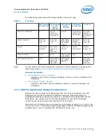
The table below summarizes the characteristics of each I/O type.
Table 7.
I/O Types
HPS Dedicated
Function Pins
HPS Dedicated
I/O with
loaner
capability
HPS External
Memory
Interface
HPS General
Purpose Input
FPGA I/O
Number of Available I/O
11
Up to 67
(Cyclone V
SoC) and 94
(Arria V SoC)
Up to 86
14 (except for
Cyclone V SoC
U19 package )
Up to 288
(Cyclone V
SoC) and Up to
592 (Arria V
SoC)
Voltages Supported
3.3V, 3.0V,
2.5V, 1.8V,
1.5V
3.3V, 3.0V,
2.5V, 1.8V,
1.5V
LVDS I/O for
DDR3, DDR2
and LPDDR2
protocols
Same as the
I/O bank
voltage used
for HPS EMIF
3.3V, 3.0V,
2.5V, 1.8V,
1.5V, 1.2V
Purpose
Clock, Reset,
HPS JTAG
Boot source,
High speed
HPS
peripherals
Connect to
SDRAM
General
Purpose Input
General
Purpose I/O
Timing Constraints
Fixed
Fixed
Fixed for legal
combinations
Fixed
User defined
Recommended Peripherals
JTAG
QSPI, NANDx8,
eMMC, SD/
MMC, UART,
USB, EMAC
DDR3, DDR2
and LPDDR2
SDRAM
GPI
Slow speed
peripherals
(I
2
C, SPI,
EMAC-MII)
Note:
You can access the timing information to perform off-chip analysis by reviewing the
HPS timing in the
or
Related Information
•
I/O Features in Cyclone V Devices
Chapter in the Cyclone V Device Handbook, Volume 1: Device Interfaces and
Integration
•
I/O Features in Arria V Devices
Chapter in the Arria V Device Handbook, Volume 1: Device Interfaces and
Integration
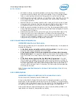
3.2.1. HPS Pin Assignment Design Considerations
Because the HPS contains more peripherals than can all be connected to the HPS
Dedicated I/O, the HPS component in Platform Designer (Standard) offers pin
multiplexing settings as well as the option to route most of the peripherals into the
FPGA fabric. Any unused pins for the HPS Dedicated I/O with loaner capability
meanwhile can be used as general purpose I/O by the FPGA.
Note that a HPS I/O Bank can only support a single supply of either 1.2V, 1.35V, 1.5V,
1.8V, 2.5V, 3.0V, or 3.3V power supply, depending on the I/O standard required by the
specified bank. 1.35V is supported for HPS Row I/O bank only.
3. Design Guidelines for HPS portion of SoC FPGAs
AN-796 | 2018.06.18
AN 796: Cyclone V and Arria V SoC Device Design Guidelines
17

