3.4.2. HPS SDRAM I/O Locations
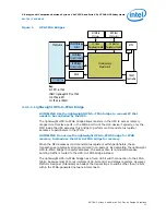
The Cyclone V and Arria V SoC HPS External Memory Interface I/O locations are fixed,
depending on the type of memory used. You can refer to the device Pin Out files,
under the “
HMC Pin Assignment for DDR3/DDR2
” and “
HMC Pin Assignment
for LPDDR2
” for exact I/O pins used by the respective memory interface pins.
Note:
Unused HPS External Memory Interface I/O Pins cannot be assigned to HPS
Peripherals, or used by the FPGA as Loaner IO.
Note:
The smallest Cyclone V SoC package U19 (484 pin count) has narrower HPS SDRAM
width (32-bit) compared to larger packages (40-bit). Refer to the
Interfaces in Cyclone V Devices"
chapter in Cyclone V Device Handbook Volume 1:
Device Interfaces and Integration for more information.
Related Information
Documentation: Pin-Out Files for Intel FPGA Devices
3.4.3. Integrating the HPS EMIF with the SoC FPGA Device
Consider the following when integrating the Cyclone V or Arria V SoC HPS EMIF with
the rest of the SoC system design.
GUIDELINE: Follow the guidelines for optimizing bandwidth for all masters
accessing the HPS SDRAM
Accesses to SDRAM connected to the HPS EMIF go through the L3 Interconnect
(except for FPGA-to-SDRAM bridge). When designing and configuring high bandwidth
DMA masters and related buffering in the FPGA core, refer to
page 24. The principles covered in that section apply to all high bandwidth DMA
masters (for example DMA controller components, integrated DMA controllers in
custom peripherals) and related buffering in the FPGA core that access HPS resources
(for example HPS SDRAM) through the FPGA-to-SDRAM and FPGA-to-HPS bridge
ports, not just tightly-coupled HPS hardware accelerators.
3.4.4. HPS Memory Debug
The Cyclone V / Arria V HPS EMIF do not support the external memory interface
toolkit. To debug the HPS EMIF, you can change the settings inside the preloader
software to enable Runtime Calibration Report and Debug Level info. In addition, you
can use the preloader software to check the status of HPS SDRAM PLL.
Using the Preloader To Debug the HPS SDRAM
information.
3. Design Guidelines for HPS portion of SoC FPGAs
AN-796 | 2018.06.18
AN 796: Cyclone V and Arria V SoC Device Design Guidelines
23


