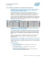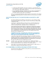
Figure 4.
RGMII
TX_CLK
TX_CTL
TXD3, TXD2, TXD1, TXD0
RX_CLK
RX_CTL
RXD3, RXD2, RXD1, RXD0
MDC
MDIO
TXC
TX_CTL
TXD[3:0]
RXC
RX_CTL
RXD[3:0]
MDC
MDIO
HPS EMAC
RGMII PHY
I/O Pin Timing
This section addresses RGMII interface timing from the perspective of meeting
requirements in the 1000 Mbps mode. The interface timing margins are most
demanding in 1000 Mbps mode, thus it is the only scenario we consider here.
At 125 MHz, the period is 8 ns, but because both edges are used, the effective period
is only 4 ns. The
TX
and
RX
busses are completely separate and source synchronous,
simplifying timing. The RGMII spec calls for
CLK
to be delayed from
DATA
at the
receiver in either direction by a minimum 1.0 ns and a maximum 2.6 ns.
In other words, the
TX_CLK
from the MAC to the PHY must be delayed from the
output to the PHY input and the
RX_CLK
from the PHY output to the MAC input. The
signals are transmitted source synchronously within the +/-500 ps RGMII skew spec in
each direction as measured at the output pins. The minimum delay needed in each
direction is 1ns but it is recommended to target a delay of 1.5 ns to 2 ns to keep
timing margin.
Transmit path setup/hold
Only setup and hold for
TX_CLK
to
TX_CTL
and
TXD[3:0]
matter for transmit. The
Cyclone V/Arria V HPS Dedicated I/O does not feature programmable delay.
For
TX_CLK
from the Cyclone V/Arria V SoC, you must introduce the 1.0 ns PHY
minimum input setup time in the RGMII spec. It is strongly recommended to increase
this to delay to 1.5 ns to 2.0 ns. Many PHYs offer programmable skew, and some
support RGMII 2.0 which defaults to skew enabled on both transmit and receive
datapaths.
Between PHY delay and FPGA I/O delay features, you must ensure either 2 ns of delay
to
CLK
versus
CTL
and
D[3:0]
or 1.2 ns typical minimum setup skew typical of most
PHYs. Consult the datasheet for your PHY vendor for more details.
4. Board Design Guidelines for SoC FPGAs
AN-796 | 2018.06.18
AN 796: Cyclone V and Arria V SoC Device Design Guidelines
38

