background image

B. Additional Information

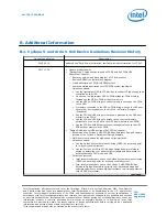
B.1. Cyclone V and Arria V SoC Device Guidelines Revision History

Document Version

Description

2018.06.18

Updated the "Early Power Estimation" section to include information for CVSoC

L.

2017.12.22

• Update product names
• "Background: Comparison between SoC FPGA and SoC FPGA HPS

Subsystem" chapter:
— Remove overview and block diagram of L3 interconnect
— Remove SDRAM controller block diagram
— Clarify description of FPGA-to-SDRAM access
— Remove detailed descriptions of HPS-FPGA system topologies
— Guidelines added:

• Use the lightweight HPS-to-FPGA bridge to connect IP that needs to be

controlled by the HPS.

• Do not use the lightweight HPS-to-FPGA bridge for FPGA memory.

Instead use the HPS-to-FPGA bridge for memory.

• Use the HPS-to-FPGA bridge to connect memory hosted by the FPGA

to the HPS..

• If memory connected to the HPS-to-FPGA bridge is used for HPS boot,

ensure that its slave address is set to 0x0 in Platform Designer

(Standard).

• Use the FPGA-to-HPS bridge for cacheable accesses to the HPS from

masters in the FPGA.

• Use the FPGA-to-HPS bridge to access cache-coherent memory,

peripherals, or on-chip RAM in the HPS from masters in the FPGA.

• Use the FPGA-to-SDRAM ports for non-cacheable access to the HPS

SDRAM from masters in the FPGA.

• "Design Guidelines for HPS portion of SoC FPGAs" chapter:

— Recommend the Cyclone V HPS-FPGA Bridge Reference Design Example

instead of the Cyclone V Datamover Design Example

— GPIO not recommended for high-speed serial interfaces
— Guidelines added:

• Use the Golden System Reference Design (GSRD) as a starting point

for a loosely coupled system.

• Use the Cyclone V HPS-to-FPGA Bridge Design Example reference

design to determine your optimum burst length and data-width for

accesses between FPGA logic and HPS.

— Guidelines removed:

• Intel recommends that you use the Golden System Reference Design

(GSRD) as a starting point for a loosely coupled system.

• Intel recommends that you use the Cyclone V HPS-FPGA Bridge

Reference Design Example to optimize your hardware design and

software solutions to achieve high performance real time application

with HPS ARM processor.

continued...   

AN-796 | 2018.06.18

Intel Corporation. All rights reserved. Intel, the Intel logo, Altera, Arria, Cyclone, Enpirion, MAX, Nios, Quartus

and  Stratix  words  and  logos  are  trademarks  of  Intel  Corporation  or  its  subsidiaries  in  the  U.S.  and/or  other

countries.  Intel  warrants  performance  of  its  FPGA  and  semiconductor  products  to  current  specifications  in

accordance with Intel's standard warranty, but reserves the right to make changes to any products and services

at any time without notice. Intel assumes no responsibility or liability arising out of the application or use of any

information,  product,  or  service  described  herein  except  as  expressly  agreed  to  in  writing  by  Intel.  Intel

customers  are  advised  to  obtain  the  latest  version  of  device  specifications  before  relying  on  any  published

information and before placing orders for products or services.

*Other names and brands may be claimed as the property of others.

ISO

9001:2015

Registered

Summary of Contents for Arria V

Page 1: ...AN 796 Cyclone V and Arria V SoC Device Design Guidelines Updated for Intel Quartus Prime Design Suite 18 0 Subscribe Send Feedback AN 796 2018 06 18 Latest document on the web PDF HTML ...

Page 2: ...cking and Reset Design Considerations 19 3 3 1 HPS Clock Planning 20 3 3 2 Early Pin Planning and I O Assignment Analysis 20 3 3 3 Pin Features and Connections for HPS JTAG Clocks Reset and PoR 20 3 3 4 Internal Clocks 21 3 4 HPS EMIF Design Considerations 21 3 4 1 Considerations for Connecting HPS to SDRAM 21 3 4 2 HPS SDRAM I O Locations 23 3 4 3 Integrating the HPS EMIF with the SoC FPGA Device...

Page 3: ... of Your Software Development Platform 49 5 1 2 Selecting an Operating System for Your Application 52 5 1 3 Assembling your Software Development Platform for Linux 53 5 1 4 Assembling a Software Development Platform for a Bare Metal Application 57 5 1 5 Assembling your Software Development Platform for a Partner OS or RTOS 58 5 1 6 Choosing Boot Loader Software 58 5 1 7 Selecting Software Tools fo...

Page 4: ...Guidelines Related Information Arria V Hard Processor System Technical Reference Manual Cyclone V Hard Processor System Technical Reference Manual Intel MAX 10 FPGA Design Guidelines AN 796 2018 06 18 Intel Corporation All rights reserved Intel the Intel logo Altera Arria Cyclone Enpirion MAX Nios Quartus and Stratix words and logos are trademarks of Intel Corporation or its subsidiaries in the U ...

Page 5: ...oller on page 24 Optimizing DMA Master Bandwidth through HPS Interconnect on page 24 Timing Closure for FPGA Accelerators on page 24 Managing Coherency for FPGA Accelerators Cache Coherency on page 25 Coherency between FPGA Logic and HPS Accelerator Coherency Port ACP on page 25 Data Size Impacts ACP Performance on page 25 FPGA Access to ACP via AXI or Avalon MM on page 26 Data Alignment for ACP a...

Page 6: ...x Device Tree Design Considerations on page 56 Assemble your Software Development Platform for Bare metal Application Assembling a Software Development Platform for a Bare Metal Application on page 57 Assemble your Software Development Platform for Partner OS RTOS Application Assembling your Software Development Platform for a Partner OS or RTOS on page 58 Choose the Boot Loader Software Choosing ...

Page 7: ...ions for Connecting Device I O to HPS Peripherals and Memory on page 16 HPS Clocks and Reset Considerations HPS clocks and cold and warm reset considerations HPS Clocking and Reset Design Considerations on page 19 HPS EMIF Considerations Usage of the HPS EMIF controller and related considerations HPS EMIF Design Considerations on page 21 FPGA Accelerator Design Considerations Design considerations...

Page 8: ...n design considerations for HPS and FPGA power supplies power analysis and power optimization HPS Power Design Considerations on page 32 Board design guidelines for HPS interfaces Includes EMAC USB QSPI SD MMC NAND UART and I2C Design Guidelines for HPS Interfaces on page 36 1 Overview of the Design Guidelines for Cyclone V SoC FPGAs and Arria V SoC FPGAs AN 796 2018 06 18 AN 796 Cyclone V and Arr...

Page 9: ...your application needs including GPL requirements and features Choosing Boot Loader Software on page 58 Boot and Configuration Design Considerations Boot source boot clock boot fuses configuration flows Boot and Configuration Design Considerations on page 28 HPS ECC Considerations ECC for external SDRAM interface L2 cache data memory flash memory HPS ECC Design Considerations on page 61 HPS SDRAM ...

Page 10: ...ntroller Bus Architecture AMBA Advanced eXtensible Interface AXI Their purpose determines the direction of each bridge 1 You can only assign a maximum of 71 HPS I O as Loaner I O to the FPGA For a detailed comparison between the HPS subsystem for Cyclone V SoC and Arria V SoC refer to Differences Among Intel SoC Device Families AN 796 2018 06 18 Intel Corporation All rights reserved Intel the Inte...

Page 11: ...atus register accesses to peripherals in the FPGA GUIDELINE Do not use the lightweight HPS to FPGA bridge for FPGA memory Instead use the HPS to FPGA bridge for memory When the MPU accesses control and status registers within peripherals these transactions are typically strongly ordered non posted By dedicating the lightweight HPS to FPGA bridge to register accesses the access time is minimized be...

Page 12: ... FPGA The FPGA to HPS bridge allows masters implemented in the FPGA fabric to access memory and peripherals inside the HPS This bridge supports 32 64 and 128 bit datapaths so that you can adjust it to be as wide as the widest master implemented in the FPGA GUIDELINE Use the FPGA to HPS bridge to access cache coherent memory peripherals or on chip RAM in the HPS from masters in the FPGA Although th...

Page 13: ...FPGA to HPS SDRAM Port Utilization Bus Protocol Command Ports Read Data Ports Write Data Ports 32 or 64 bit AXI 2 1 1 128 bit AXI 2 2 2 256 bit AXI 2 4 4 32 or 64 bit Avalon MM 1 1 1 128 bit Avalon MM 1 2 2 256 bit Avalon MM 1 4 4 32 or 64 bit Avalon MM write only 1 0 1 128 bit Avalon MM write only 1 0 2 256 bit Avalon MM write only 1 0 4 32 or 64 bit Avalon MM read only 1 1 0 128 bit Avalon MM re...

Page 14: ...DMA Considerations on page 24 section of this document The principles covered in that section apply to all high bandwidth DMA masters for example Platform Designer Standard DMA Controller components integrated DMA controllers in custom peripherals and related buffering in the FPGA core that access HPS resources for example HPS SDRAM through the FPGA to SDRAM and FPGA to HPS bridge ports not just t...

Page 15: ...2 Determining your SoC FPGA Topology To determine which system topology best suits your application you must first determine how to partition your application into hardware and software GUIDELINE Profile your software to identify functions for hardware acceleration Use any good profiling tool such as DS 5 streamline profiler to identify functions that are good candidates for hardware acceleration ...

Page 16: ...mmary Pin Type Purpose HPS Dedicated Function Pins Each I O has only one function and cannot be used for other purposes HPS Dedicated I O with loaner capability These I Os are primarily used by the HPS but can be used on an individual basis by the FPGA if the HPS is not using them HPS External Memory Interface EMIF I O These I Os are used for connecting to the HPS external memory interface EMIF Re...

Page 17: ...formation to perform off chip analysis by reviewing the HPS timing in the Cyclone V Device Datasheet or Arria V Device Datasheet Related Information I O Features in Cyclone V Devices Chapter in the Cyclone V Device Handbook Volume 1 Device Interfaces and Integration I O Features in Arria V Devices Chapter in the Arria V Device Handbook Volume 1 Device Interfaces and Integration 3 2 1 HPS Pin Assig...

Page 18: ...terface in the Platform Designer Standard HPS Component for Cyclone V Arria V These pins are then exposed as part of the Platform Designer Standard HPS Component Conduit Interface and can be individually assigned at the top level of the design 3 2 2 HPS I O Settings Constraints and Drive Strengths GUIDELINE Ensure that you have I O settings for the HPS Dedicated I O drive strength I O standard wea...

Page 19: ...nPOR HPS_nRST and HPS_PORSEL HPS_CLK1 sources the Main PLL that generates the clocks for the MPU L3 L4 sub systems debug sub system and the Flash controllers It can also be programmed to drive the Peripheral and SDRAM PLLs HPS_CLK2 meanwhile can be used as an alternative clock source to the Peripheral and the SDRAM PLLs HPS_nPOR provides a cold reset input and HPS_nRST provides a bidirectional war...

Page 20: ...ctions for HPS JTAG Clocks Reset and PoR GUIDELINE With the HPS in use powered supply a free running clock on HPS_CLK1 for SoC device HPS JTAG access Access to the HPS JTAG requires an active clock source driving HPS_CLK1 GUIDELINE When daisy chaining the FPGA and HPS JTAG for a single device ensure that the HPS JTAG is first device in the chain located before the FPGA JTAG Placing the HPS JTAG be...

Page 21: ...erations A critical component of the HPS subsystem is the external SDRAM memory For Cyclone V and Arria V SoC device the HPS has a dedicated SDRAM Subsystem that interfaces with the HPS External Memory Interface I O Review the following guidelines to properly design the interface between the memory and the HPS These guidelines are essential to successfully connecting external SDRAM to the HPS The ...

Page 22: ... to compare supported external memory interface types configurations and maximum performance characteristics in Intel FPGA and SoC devices First filter the Family to select only Cyclone V Arria V SoC device Then follow on by using the filter on Interface Type to choose only HPS Hard Controller GUIDELINE Ensure that in the HPS Component the Memory Clock Frequency is supported by the device speed gr...

Page 23: ...idelines for optimizing bandwidth for all masters accessing the HPS SDRAM Accesses to SDRAM connected to the HPS EMIF go through the L3 Interconnect except for FPGA to SDRAM bridge When designing and configuring high bandwidth DMA masters and related buffering in the FPGA core refer to DMA Considerations on page 24 The principles covered in that section apply to all high bandwidth DMA masters for ...

Page 24: ...ng bandwidth through the interconnect GUIDELINE Utilize the Cyclone V FPGA to HPS Bridge Design Example to tune for performance The Cyclone V FPGA to HPS Bridge Design Example is a useful platform for modeling specific data traffic access patterns between the FPGA and HPS resources The example design includes a utility that can select the datapaths between endpoints select transaction characterist...

Page 25: ...tem level within the MPU subsystem The snoop control unit SCU built into the MPU subsystem maintains cache coherency between the two L1 data caches using the modified exclusive shared invalid MESI coherency protocol 3 6 2 Coherency between FPGA Logic and HPS Accelerator Coherency Port ACP The accelerator coherency port ACP of the SCU provides a means for other masters in the system including logic...

Page 26: ...ith the L2 cache ECC logic if the access is aligned to 8 byte boundaries and the master performs bursts of size 2 4 8 or 16 Data resizing can also occur within the FPGA to HPS bridge GUIDELINE The simplest way to ensure that accesses from the FPGA meets the L2 cache ECC requirements is to implement 64 bit masters in the FPGA fabric and configure the FPGA to HPS bridge to expose a 64 bit slave port...

Page 27: ...e also capable of being used simultaneously with the HPS tools that communicate over JTAG There are two JTAG interfaces on the Cyclone V Arria V SoC device The first interface is connected to the FPGA side of the device while the second interface is connected to the HPS debug access port DAP Related Information Design Debugging Using In System Sources and Probes chapter of the Intel Quartus Prime ...

Page 28: ...bric Each possible boot source has its own strengths AN 796 2018 06 18 Intel Corporation All rights reserved Intel the Intel logo Altera Arria Cyclone Enpirion MAX Nios Quartus and Stratix words and logos are trademarks of Intel Corporation or its subsidiaries in the U S and or other countries Intel warrants performance of its FPGA and semiconductor products to current specifications in accordance...

Page 29: ...Is the flash device compatible with the HPS boot ROM The HPS can only boot from flash devices supported in the boot ROM Is the device verified to work and supported by software like Preloader U Boot and Linux For supported devices Intel provides the Preloader U Boot and Linux software For other devices this software must be developed by the user Is the flash device supported by the HPS Flash Progr...

Page 30: ...values even if the end product requires just one CSEL setting If possible design the board in such a way that the CSEL configuration can be varied even if a single value will eventually be used This configurability may be useful for debugging and could be done by resistors jumpers or switches 4 2 1 6 Selecting NAND Flash Devices GUIDELINE Select a NAND flash that is ONFI 1 0 compliant When booting...

Page 31: ...hat some devices do not have a reset pin In such a case you must power cycle the flash by other means for example with a MOSFET Pay attention to minimum required reset pulse duration 4 2 1 9 Selecting QSPI Flash Devices GUIDELINE For bare metal applications avoid using a QSPI flash device larger than 16 MB QSPI flash devices of 16 MB or less always support three byte addressing Therefore they are ...

Page 32: ...ll the device I O default to an input tri state mode of operation The boot ROM configures the dedicated boot I O based on the sampled BSEL pins 4 2 3 Reference Materials Refer to the following reference materials for additional information Related Information Intel SoC FPGA Embedded Development Suite User Guide Support tab on Cyclone V SoCs Cyclone V SoC documentation Support tab on Arria V SoCs A...

Page 33: ...h CPU allow you to select from a list of industry standard benchmarks to model CPU utilization in your application You can also select Custom for defining a unique set of CPU utilization parameters across the ALUs and cache memories GUIDELINE Use the HPS worksheet to update the HPS SDRAM Type Frequency and Width Note that the selection of SDRAM type also updates the I O voltage for Bank 6A to 6B G...

Page 34: ...or using the I2C connection from the HPS 4 3 2 2 Consider Desired HPS Boot Clock Frequency Cyclone V Arria V SoC devices support a HPS boot clock from 10 50 MHz in PLL bypass mode and up to 400MHz in PLL Locked mode During power up or cold reset the boot ROM samples the value of the CSEL pins and if needed configure the HPS PLL to provide a faster boot clock frequency Refer to the table with CSEL ...

Page 35: ... Related Information Arria V and Cyclone V Design Guidelines Cyclone V Device Handbook Arria V Device Handbook 4 3 4 Power Analysis and Optimization Follow the guidelines in the Power Analysis and Optimization section of the Arria V and Cyclone V Design Guidelines In addition consider the following options for the HPS portion of the device Processor and memory clock speeds The biggest contribution...

Page 36: ...1 HPS EMAC PHY Interfaces When configuring an HPS component for EMAC peripherals within Platform Designer Standard you must select from one of the following supported PHY interfaces for each EMAC instance Reduced Gigabit Media Independent Interface RGMII using dedicated I O Media Independent Interface MII interface to FPGA fabric Gigabit Media Independent Interface GMII interface to FPGA fabric An...

Page 37: ...face is not supported when routing through the HPS Dedicated I O RMII interface however is supported when routing through the FPGA fabric Related Information Introduction to the HPS Component chapter of the Cyclone V Hard Processor System Technical Reference Manual Introduction to the HPS Component chapter of the Arria V Hard Processor System Technical Reference Manual Golden System Reference Desi...

Page 38: ...mitted source synchronously within the 500 ps RGMII skew spec in each direction as measured at the output pins The minimum delay needed in each direction is 1ns but it is recommended to target a delay of 1 5 ns to 2 ns to keep timing margin Transmit path setup hold Only setup and hold for TX_CLK to TX_CTL and TXD 3 0 matter for transmit The Cyclone V Arria V HPS Dedicated I O does not feature prog...

Page 39: ...PS EMAC GUIDELINE Specify the PHY interface transmit clock frequency when configuring the HPS component within Platform Designer Standard For either GMII or MII including adapting to other PHY interfaces specify the maximum transmit path clock frequency for the HPS EMAC PHY interface 125 MHz for GMII 25 MHz for MII This configuration results in the proper clock timing constraints being applied to ...

Page 40: ...ning 20 ns setup timing budget it may be necessary to retime the transmit data and control to the rising edge of the phy_txclk_o clock output registers in the FPGA fabric for MII mode transmit data and control 4 5 1 2 2 Adapting to RGMII It is possible to adapt the GMII HPS EMAC PHY signals to an RGMII PHY interface at the FPGA I O pins using logic in the FPGA While it is possible to design custom...

Page 41: ...d 100 Mbps modes of operation The RMII transmit and receive datapaths are 2 bits wide At 10 Mbps transmit and receive data and control are held stable for 10 clock cycles of the 50 MHz REF_CLK You must provide adaptation logic in the FPGA fabric to adapt between the HPS EMAC MII and external RMII PHY interfaces 4 bits 25 MHz 2 5 MHz to from 2 bits 50 MHz 10x oversampled in 10 Mbps mode GUIDELINE P...

Page 42: ... bus turnaround period When the MAC writes to the PHY the data is launched on the falling edge meaning there is 200 ns 10 ns 190 ns for flight time signal settling and setup at the receiver Because data is not switched until the following negative edge there is also 200 ns of hold time These requirements are very easy to meet with almost any board topology When the MAC reads from the PHY the PHY i...

Page 43: ...xternal clock is the source The interface between the ULPI MAC and PHY on the Cyclone V Arria V SoC consists of DATA 7 0 DIR and NXT from the MAC to the PHY and STP from the MAC to the PHY Lastly a static clock of 60 MHz is driven from the PHY and is required for operation including some register accesses from the HPS to the USB MAC Ensure the PHY manufacturer recommendations for RESET and power u...

Page 44: ... design uses QSPI flash with 4 byte addressing design the board to ensure that the QSPI flash is reset or power cycled whenever the HPS is reset The HPS boot ROM on Cyclone V and Arria V runs in 3 byte address mode by default If the QSPI flash is switched to 4 byte addressing during operation ensure that it is returned to its default 3 byte addressing mode whenever the HPS is reset Otherwise the H...

Page 45: ...sfer mode as well as normal operation SD cards initially operate at 400 KHz maximum when they are going through the ID process After that there is a data transfer mode during which the clock can operate up to 12 5 MHz In normal operation the clock can operate up to 50 MHz The Boot ROM takes care to ensure that clocking is properly configured during ID and transfer modes Refer to the CSEL Settings ...

Page 46: ...ytes 24 bit correction You cannot export the NAND interface to FPGA Note Refer to Supported Flash Devices for Cyclone V and Arria V SoC for a list of supported NAND devices 4 5 6 UART Interface Design Guidelines GUIDELINE Properly connect flow control signals when routing the UART signals through the FPGA fabric When routing UART signals through the FPGA the flow control signals are available If f...

Page 47: ...O 4 5 8 SPI Interface Design Guidelines GUIDELINE Consider routing SPI slave signals to FPGA fabric Due to an erratum in the Cyclone V Arria V SoC device the SPI output enable is not connected to the SPI HPS pins As a result the HPS SPIS_TXD pin cannot be tri stated by setting the slv_oe bit bit 10 in the ctrlr0 register to 1 Routing the SPI Slave signals to FPGA exposes the output enable signal a...

Page 48: ...ect is mapped to GPIO Related Information ctrlr0 For details about the ctrlr0 scph and ctrlr0 scpol bits in the Cyclone V HPS refer to ctrlr0 in the SPI Master chapter of the Cyclone V Hard Processor System Technical Reference Manual ctrlr0 For details about the ctrlr0 scph and ctrlr0 scpol bits in the Arria V HPS refer to ctrlr0 in the SPI Master chapter of the Arria V Hard Processor System Techn...

Page 49: ... Metal Applications Drivers Write Modify Linux Applications Drivers Write Modify RT OS Applications Drivers Hardware Software Bare Metal AN 796 2018 06 18 Intel Corporation All rights reserved Intel the Intel logo Altera Arria Cyclone Enpirion MAX Nios Quartus and Stratix words and logos are trademarks of Intel Corporation or its subsidiaries in the U S and or other countries Intel warrants perfor...

Page 50: ...design for the Cyclone V SoC Arria V SoC Development Kit The GHRD has connections to a boot source SDRAM memory and other peripherals on the development board For every new released version of SoC EDS the GHRD is included in the SoC EDS tools The GHRD is regression tested with every major release of the Intel Quartus Prime Design Software and includes the latest bug fixes for known hardware issues...

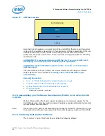
Page 51: ...rocessor System FPGA Fabric I Cache D Cache I Cache D Cache CPU0 CPU1 ARM Coretex A9 MPCore The GHRD has a minimal set of peripherals in the FPGA fabric because the HPS provides a substantial selection of peripherals HPS to FPGA and FPGA to HPS interfaces are configured to a 64 bit data width GUIDELINE Intel recommends that you use the latest GHRD as a baseline for new SoC FPGA hardware projects Y...

Page 52: ... familiarize yourself with the features and support services offered by the commercial and open source operating systems available for the SoC FPGA Intel s OS partners industry websites are a good source of information you can use to help make your selection There are a number of misconceptions when it comes to real time performance of operating systems versus bare metal applications For a Cortex ...

Page 53: ...essor affinity This means that each task thread can be assigned to run on a specific core This feature allows the software developer to better control the workload distribution for each Cortex A9 core and making the system more responsive as an alternative to AMP GUIDELINE Familiarize yourself with the performance and optimizations available in commercial operating systems to see if an SMP enabled...

Page 54: ...ftware development platform it is recommended that you use the GSRD as a baseline project then modify it to suit your application needs The GSRDs target the Intel SoC Development Boards and are provided both in source and pre compiled form They can be obtained from GSRD User Manuals GUIDELINE It is recommended that all new projects use the latest version of GSRD as a baseline 5 1 3 2 GSRD for Linu...

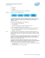
Page 55: ... 3 GSRD for Linux Build Flow The figure below presents a detailed build flow for the GSRD Refer to the GSRD User Manuals link given below for more details 5 Embedded Software Design Guidelines for SoC FPGAs AN 796 2018 06 18 AN 796 Cyclone V and Arria V SoC Device Design Guidelines 55 ...

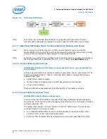
Page 56: ...be manually edited Related Information GSRD User Manuals 5 1 3 4 Linux Device Tree Design Considerations The Linux Device Tree is a data structure that describes the underlying hardware to the Linux operating system kernel By passing this data structure the OS kernel a single OS binary may be able to support many variations of hardware This flexibility is particularly important when the hardware i...

Page 57: ...GSRD for Linux Refer to the DeviceTree Generator User Guide link given below for more details about the Linux Device Tree Generator Related Information DeviceTree Generator User Guide 5 1 4 Assembling a Software Development Platform for a Bare Metal Application Intel hardware libraries HWLibs are low level bare metal software libraries provided with SoC EDS and various components of the HPS The HW...

Page 58: ...ing a Bare metal HwLibs Project Automatically Related Information Intel SoC FPGA Embedded Development Suite User Guide Creating a Bare metal HwLibs Project Automatically Getting Started with HwLibs Baremetal Development Design Examples Additional HWLibs examples 5 1 5 Assembling your Software Development Platform for a Partner OS or RTOS Partner OS providers offer board support packages and commer...

Page 59: ...the next stage boot image Also the header contains a CRC value used to validate the image The header can be attached to an image by using the mkimage utility that is included with SoC EDS The Bootloader has typical responsibilities that are similar with the Preloader except it does not need to bring up SDRAM Because the Bootloader is already residing in SDRAM it is not limited by the size of the O...

Page 60: ...ssemblers linkers and archivers The Arm Development Studio 5 DS 5 Intel SoC FPGA Edition includes the following software build tools ARMCC Bare metal Compiler Mentor Graphics CodeSourcery Lite GCC based bare metal Compiler Linux Linaro Compiler There are also other development tools offerings from third party providers 5 1 7 2 Select Software Debug Tools GUIDELINE Select software debug tools Arm D...

Page 61: ... Work device This means that the device is compatible with BootROM and was proven to work with at least one Bootloader but it may not be the Bootloader you need It may also not have HWLibs OS Support or HPS Flash Programmer Support 5 3 HPS ECC Design Considerations ECC is implemented throughout the entire HPS subsystem on all RAMs including the external HPS EMIF L2 cache data RAMs and all peripher...

Page 62: ...r Address Map for Arria V GUIDELINE The L1 and L2 cache must be configured as write back and write allocate for any cacheable memory region with ECC enabled For BSPs supported by the Intel SoC FPGA EDS you can configure your BSP for ECC support with the bsp editor utility For bare metal firmware refer to L2 Cache Controller Address Map in the Cortex A9 Microprocessor Unit Subsystem chapter of the ...

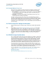
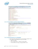
Page 63: ...S SDRAM Considerations 5 4 1 Using the Preloader To Debug the HPS SDRAM To debug the HPS EMIF you can change the settings in the preloader to enable runtime calibration report debug level information and check the status of HPS SDRAM PLL Note Refer to Building the Second Stage Bootloader in the Intel SoC FPGA Embedded Development Suite User Guide for step by step instructions for compiling the pre...

Page 64: ...or Note Example driver is only available in Intel Quartus Prime version 14 0 and later PRBS31 Data pattern Write to random address Read from random address Can select different coverage by changing parameter in spl c 5 Embedded Software Design Guidelines for SoC FPGAs AN 796 2018 06 18 AN 796 Cyclone V and Arria V SoC Device Design Guidelines 64 ...

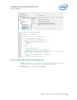
Page 65: ..._test c project_folder software spl_bsp uboot socfpga arch arm cpu armv7 socfpga sdram_test c 2 Change the test_rand_address function 5 Embedded Software Design Guidelines for SoC FPGAs AN 796 2018 06 18 AN 796 Cyclone V and Arria V SoC Device Design Guidelines 65 ...

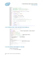
Page 66: ...Addresses 5 4 1 6 Read Write to HPS Register in Preloader Use the following function 1 writel to write to HPS register 5 Embedded Software Design Guidelines for SoC FPGAs AN 796 2018 06 18 AN 796 Cyclone V and Arria V SoC Device Design Guidelines 66 ...

Page 67: ...tialized yet 5 4 2 Access HPS SDRAM via the FPGA to SDRAM Interface The HPS bridges can be enabled from the Preloader SPL MPL or U Boot and in some cases from Linux Note Preloaders SPL and U Boot generated from SoC EDS 13 1 and later contain extra functionality and built in functions to safely enable the HPS bridges To enable the HPS FPGA to SDRAM bridge from the Preloader or U Boot follow the app...

Page 68: ...SRD v13 1 Programming FPGA from HPS Enabling HPS to FPGA Bridges from U Boot The bridge_enable_handoff command can be run from the U boot command prompt to enable bridges This command puts the HPS and SDRAM into a safe state before enabling all bridges after appropriate checks For more information refer to the KDB solution How can I enable the FPGA2SDRAM bridge on Cyclone V SoC and Arria V SoC Dev...

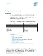
Page 69: ...Designs Reference designs and design examples for Intel FPGA products Intel FPGA Design Solutions Network Embedded Support Center Design Examples for Intel FPGA products Development Kits Daughter Cards Programming Hardware Support Intel Wiki AN 796 2018 06 18 Intel Corporation All rights reserved Intel the Intel logo Altera Arria Cyclone Enpirion MAX Nios Quartus and Stratix words and logos are tr...

Page 70: ...Related Information RocketBoards org Documentation Portal Altera Opensource RocketBoards org repository of Linux related source code RocketBoards org Boards RocketBoards org Projects Intel SoC FPGA Embedded Development Suite User Guide Download SoC EDS Getting Started tab of the Intel SoC FPGA Embedded Development Suite page A Support and Documentation AN 796 2018 06 18 AN 796 Cyclone V and Arria ...

Page 71: ...GPIO not recommended for high speed serial interfaces Guidelines added Use the Golden System Reference Design GSRD as a starting point for a loosely coupled system Use the Cyclone V HPS to FPGA Bridge Design Example reference design to determine your optimum burst length and data width for accesses between FPGA logic and HPS Guidelines removed Intel recommends that you use the Golden System Refere...

Page 72: ...or configure the SPI master to assert slave select during the transaction Ensure that the SD MMC card is reset whenever the HPS is reset For bare metal applications avoid using a QSPI flash device larger than 16 MB With a QSPI device larger than 16 MB use QSPI extended 4 byte addressing commands if supported by the device Embedded Software Design Guidelines for SoC FPGAs chapter Reference DTB for ...

Reviews: