4.5.7. I
2
C Interface Design Guidelines
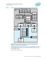
GUIDELINE: Instantiate the open-drain buffer when routing I
2
C signals
through the FPGA fabric.
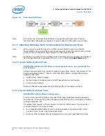
When routing I
2
C signals through the FPGA, note that the I
2
C pins from the HPS to the
FPGA fabric (
i2c*_out_data
,
i2c*_out_clk
) are not open-drain and are logic level
inverted. Thus, when you want to drive a logic level zero onto the I
2
C bus, these pins
are high. This implementation is useful as they can be used to tie to an output enable
of a tri-state buffer directly. You must use the
altiobuf
to implement the open-drain
buffer.
GUIDELINE: Ensure that the pull-ups are added to the external
SDA
and
SCL
signals in the board design.
Because the I
2
C signals are open drain, pull-ups are required to make sure that the
bus is pulled high when no device on the bus is pulling it low.
Figure 5.
I
2
C Wiring to FPGA pins
i2c*_out_data
i2c*_in_data
i2c*_out_clk
i2c*_in_clk
HPS
FPGA Fabric
FPGA I/O
4.5.8. SPI Interface Design Guidelines
GUIDELINE: Consider routing SPI slave signals to FPGA fabric
Due to an erratum in the Cyclone V/Arria V SoC device, the SPI output enable is not
connected to the SPI HPS pins. As a result, the HPS
SPIS_TXD
pin cannot be tri-
stated by setting the
slv_oe
bit (bit
10
) in the
ctrlr0
register to
1
.
Routing the SPI Slave signals to FPGA exposes the output enable signal and allows you
to connect it to an FPGA tri-state pin.
GUIDELINE: If your SPI peripheral requires the SPI master slave select to
stay low during the entire transaction period, consider using GPIO as slave
select, or configure the SPI master to assert slave select during the
transaction.
By default, the SPI master is configured with
ctrlr0.scph
= 0 and
ctrlr0.scpol
= 0, which makes the Cyclone V or Arria V HPS SPI master deassert the slave select
signal between each data word. Set
ctrlr0.scph
to 1 and
ctrlr0.scpol
to 1, to
make the SPI master assert slave select for the entire duration of the transfer.
4. Board Design Guidelines for SoC FPGAs
AN-796 | 2018.06.18
AN 796: Cyclone V and Arria V SoC Device Design Guidelines
47


