EXTERNAL BUS
14-6
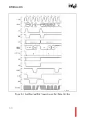
Bus accesses begin with the assertion of ADS (address/data status) during a Ta state. External
decoding logic typically uses ADS to qualify a valid address at the rising clock edge at the end of
Ta. The processor pulses ALE (address latch enable) active high for one half clock during Ta to
latch the multiplexed address on AD31:2 in external address latches. An inverted signal, ALE , is
also present for compatibility with i960 Kx processor-based companion devices.
The byte enable (BE3:0) signals denote which bytes on the 32-bit data bus will transfer data during
an access. The processor asserts byte enables during Ta and deasserts them during Tr. When the data
bus is configured for 16 bits, two byte enables become byte high enable and byte low enable and an
additional address bit A1 is provided. When the bus is configured for 8 bits, there are no byte
enables, but additional address bits A1:0 are provided. Note that the processor always drives byte
enable pins to logical 1’s during the Tr state, even when they are used as addresses.
The WIDTH1:0, D/C and W/R signals yield useful bus access information for external memory
and I/O controllers. The WIDTH1:0 signals denote programmed physical memory attributes. The
data/code pin indicates whether an access is a data transaction (1) or an instruction transaction (0).
The write/read pin indicates the direction of data flow relative to the i960 Jx processor.
WIDTH1:0, D/C and W/R change state as needed during the Ta state.
DT/R and DEN pins are used to control data transceivers. Data transceivers may be used in a
system to isolate a memory subsystem or control loading on data lines. DT/R (data
transmit/receive) is used to control transceiver direction. In the second half of the Ta state, it
transitions high for write cycles or low for read cycles. DEN (data enable) is used to enable the
transceivers. DEN is asserted during the first Tw/Td state of a bus access and deasserted during Tr.
DT/R and DEN timings ensure that DT/R does not change state when DEN is asserted.
A bus access may be either non-burst or burst. A non-burst access ends after one data transfer to a
single location. A burst access involves two to four data cycles to consecutive memory locations.
The processor asserts BLAST (burst last) to indicate the last data cycle of an access in both burst
and non-burst situations.
All i960 Jx processor wait states are controlled by the RDYRCV (ready/recover) input signal.
14.2.3
Bus Accesses
The i960 Jx microprocessor uses the bus signals to transfer data between the processor and another
component. The maximum transfer rate is achieved when performing burst accesses at the rate of
four 32-bit data words per six clocks.
Summary of Contents for i960 Jx
Page 1: ...Release Date December 1997 Order Number 272483 002 i960 Jx Microprocessor Developer s Manual ...
Page 24: ......
Page 25: ...1 INTRODUCTION ...
Page 26: ......
Page 35: ...2 DATA TYPES AND MEMORY ADDRESSING MODES ...
Page 36: ......
Page 46: ......
Page 47: ...3 PROGRAMMING ENVIRONMENT ...
Page 48: ......
Page 73: ...4 CACHE AND ON CHIP DATA RAM ...
Page 74: ......
Page 85: ...5 INSTRUCTION SET OVERVIEW ...
Page 86: ......
Page 111: ...6 INSTRUCTION SET REFERENCE ...
Page 112: ......
Page 233: ...7 PROCEDURE CALLS ...
Page 234: ......
Page 256: ......
Page 257: ...8 FAULTS ...
Page 258: ......
Page 291: ...9 TRACING AND DEBUGGING ...
Page 292: ......
Page 309: ...10 TIMERS ...
Page 310: ......
Page 324: ......
Page 325: ...11 INTERRUPTS ...
Page 326: ......
Page 369: ...12 INITIALIZATION AND SYSTEM REQUIREMENTS ...
Page 370: ......
Page 412: ......
Page 413: ...13 MEMORY CONFIGURATION ...
Page 414: ......
Page 429: ...14 EXTERNAL BUS ...
Page 430: ......
Page 468: ......
Page 469: ...15 TEST FEATURES ...
Page 470: ......
Page 493: ...A CONSIDERATIONS FOR WRITING PORTABLE CODE ...
Page 494: ......
Page 502: ......
Page 503: ...B OPCODES AND EXECUTION TIMES ...
Page 504: ......
Page 515: ...C MACHINE LEVEL INSTRUCTION FORMATS ...
Page 516: ......
Page 523: ...D REGISTER AND DATA STRUCTURES ...
Page 524: ......
Page 550: ......
Page 551: ...GLOSSARY ...
Page 552: ......
Page 561: ...INDEX ...
Page 562: ......
Page 578: ......


