EXTERNAL BUS
14-17
14
14.2.3.4
Wait States
Wait states lengthen the microprocessor’s bus cycles, allowing data transfers with slow memory
and I/O devices. The 80960Jx supports three types of wait states: address-to-data, data-to-data
and turnaround or recovery. All three types are controlled through the processor’s RDYRCV
(Ready/Recover) pin, a synchronous input.
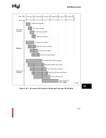
The processor’s bus states follow the state diagram in
Figure 14.1
. After the Ta state, the processor
enters the Tw/Td state to perform a data transfer. If the memory (or I/O) system is fast enough to
allow the transfer to complete during this clock (i.e., “ready”), external logic asserts RDYRCV.
The processor samples RDYRCV low on the next rising clock edge, completing the transfer; the
state is a data state. If the memory system is too slow to complete the transfer during this clock,
external logic drives RDYRCV high and the state is an address-to-data wait state. Additional wait
states may be inserted in similar fashion.
If the bus transaction is a burst, the processor re-enters the Tw/Td state after the first data transfer.
The processor continues to sample RDYRCV on each rising clock edge, adding a data-to-data wait
state when RDYRCV is high and completing a transfer when RDYRCV is low. The process
continues until all transfers are finished, with RDYRCV assertion denoting every data acquisition.
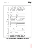
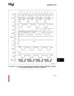
Figure 14-10
illustrates a quad word burst write transaction with wait states. There are two
address-to-data wait states single data-to-data wait states between transfers.
Summary of Contents for i960 Jx
Page 1: ...Release Date December 1997 Order Number 272483 002 i960 Jx Microprocessor Developer s Manual ...
Page 24: ......
Page 25: ...1 INTRODUCTION ...
Page 26: ......
Page 35: ...2 DATA TYPES AND MEMORY ADDRESSING MODES ...
Page 36: ......
Page 46: ......
Page 47: ...3 PROGRAMMING ENVIRONMENT ...
Page 48: ......
Page 73: ...4 CACHE AND ON CHIP DATA RAM ...
Page 74: ......
Page 85: ...5 INSTRUCTION SET OVERVIEW ...
Page 86: ......
Page 111: ...6 INSTRUCTION SET REFERENCE ...
Page 112: ......
Page 233: ...7 PROCEDURE CALLS ...
Page 234: ......
Page 256: ......
Page 257: ...8 FAULTS ...
Page 258: ......
Page 291: ...9 TRACING AND DEBUGGING ...
Page 292: ......
Page 309: ...10 TIMERS ...
Page 310: ......
Page 324: ......
Page 325: ...11 INTERRUPTS ...
Page 326: ......
Page 369: ...12 INITIALIZATION AND SYSTEM REQUIREMENTS ...
Page 370: ......
Page 412: ......
Page 413: ...13 MEMORY CONFIGURATION ...
Page 414: ......
Page 429: ...14 EXTERNAL BUS ...
Page 430: ......
Page 468: ......
Page 469: ...15 TEST FEATURES ...
Page 470: ......
Page 493: ...A CONSIDERATIONS FOR WRITING PORTABLE CODE ...
Page 494: ......
Page 502: ......
Page 503: ...B OPCODES AND EXECUTION TIMES ...
Page 504: ......
Page 515: ...C MACHINE LEVEL INSTRUCTION FORMATS ...
Page 516: ......
Page 523: ...D REGISTER AND DATA STRUCTURES ...
Page 524: ......
Page 550: ......
Page 551: ...GLOSSARY ...
Page 552: ......
Page 561: ...INDEX ...
Page 562: ......
Page 578: ......


