INDEX
Index-4
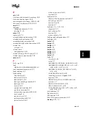
comparison instructions, overview
compare and increment or decrement instructions
5-13
test condition instructions
5-13
concmpi
6-38
concmpo
6-38
conditional branch instructions
3-19
conditional fault instructions
5-17
control registers
3-1
,
3-7
memory-mapped
3-6
overview
1-6
control table
3-1
,
3-7
,
3-12
alignment
3-15
Control Table Valid (CTV) bit
13-6
core architecture
and software portability
A-1
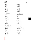
D
DAB
9-10
Data Address Breakpoint (DAB) Register Format
9-10
Data Address Breakpoint (DAB) registers
9-9
programming
9-8
data alignment in external memory
3-15
data cache
cache coherency and non-cacheable accesses
4-9
coherency
I/O and bus masters
4-10
control instruction
6-40
described
4-6
enabling and disabling
4-6
fill policy
1-4
,
4-8
overview
1-4
partial-hit multi-word data accesses
4-7
visibility
4-10
write policy
4-8
Data Cache Enable (DCEN) bit
13-12
data control peripheral units
A-7
data movement instructions
5-5
load address instruction
5-6
load instructions
5-5
move instructions
5-6
data RAM
3-16
Data Register
timing diagram
15-18
data structures
control table
3-1
,
3-7
,
3-12
fault table
3-1
,
3-12
Initialization Boot Record (IBR)
3-1
,
3-11
interrupt stack
3-1
,
3-12
interrupt table
3-1
,
3-12
literals
3-4
local stack
3-1
Process Control Block (PRCB)
3-1
,
3-11
supervisor stack
3-1
,
3-12
system procedure table
3-1
,
3-12
user stack
3-12
data types
bits and bit fields
2-3
integers
2-2
literals
2-4
ordinals
2-2
supported
2-1
triple and quad words
2-3
dcctl
3-23
,
4-6
,
4-10
,
6-40
DCEN bit, see Data Cache Enable (DCEN) bit
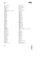
debug
overview
9-1
debug instructions
5-18
decoupling capacitors
12-36
Default Logical Memory Configuration (DLMCON)
register
13-3
DLMCON.be bit
4-4
design considerations
high frequency
12-38
interference
12-40
latchup
12-39
line termination
12-38
Device ID register
15-6
device ID Register
12-22
device ID register
D-23
DEVICEID register location
3-3
divi
6-47
divide integer instruction
6-47
divide ordinal instruction
6-47
divo
6-47
DLMCON registers
Summary of Contents for i960 Jx
Page 1: ...Release Date December 1997 Order Number 272483 002 i960 Jx Microprocessor Developer s Manual ...
Page 24: ......
Page 25: ...1 INTRODUCTION ...
Page 26: ......
Page 35: ...2 DATA TYPES AND MEMORY ADDRESSING MODES ...
Page 36: ......
Page 46: ......
Page 47: ...3 PROGRAMMING ENVIRONMENT ...
Page 48: ......
Page 73: ...4 CACHE AND ON CHIP DATA RAM ...
Page 74: ......
Page 85: ...5 INSTRUCTION SET OVERVIEW ...
Page 86: ......
Page 111: ...6 INSTRUCTION SET REFERENCE ...
Page 112: ......
Page 233: ...7 PROCEDURE CALLS ...
Page 234: ......
Page 256: ......
Page 257: ...8 FAULTS ...
Page 258: ......
Page 291: ...9 TRACING AND DEBUGGING ...
Page 292: ......
Page 309: ...10 TIMERS ...
Page 310: ......
Page 324: ......
Page 325: ...11 INTERRUPTS ...
Page 326: ......
Page 369: ...12 INITIALIZATION AND SYSTEM REQUIREMENTS ...
Page 370: ......
Page 412: ......
Page 413: ...13 MEMORY CONFIGURATION ...
Page 414: ......
Page 429: ...14 EXTERNAL BUS ...
Page 430: ......
Page 468: ......
Page 469: ...15 TEST FEATURES ...
Page 470: ......
Page 493: ...A CONSIDERATIONS FOR WRITING PORTABLE CODE ...
Page 494: ......
Page 502: ......
Page 503: ...B OPCODES AND EXECUTION TIMES ...
Page 504: ......
Page 515: ...C MACHINE LEVEL INSTRUCTION FORMATS ...
Page 516: ......
Page 523: ...D REGISTER AND DATA STRUCTURES ...
Page 524: ......
Page 550: ......
Page 551: ...GLOSSARY ...
Page 552: ......
Page 561: ...INDEX ...
Page 562: ......
Page 578: ......


