CACHE AND ON-CHIP DATA RAM
4-2
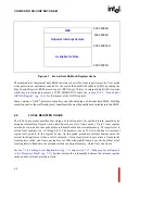
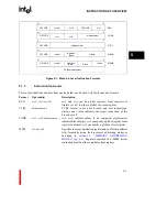
Figure 4-1. Internal Data RAM and Register Cache
The remainder of the internal data RAM can always be written from supervisor mode. User mode
write protection is optionally selected for the rest of the data RAM (40H to 3FFH) by setting the
Bus Control Register RAM protection bit (BCON.irp). Writes to internal data RAM locations
while they are protected generate a TYPE.MISMATCH fault. See
section 13.4.1, “Bus Control
(BCON) Register” (pg. 13-6)
, for the format of the BCON register.
Some versions of i960
®
processor compilers can take advantage of internal data RAM. Profiling
compilers, such as those offered by Intel, can allocate the most frequently used variables into this RAM.
4.2
LOCAL REGISTER CACHE
The i960 Jx processor provides fast storage of local registers for call and return operations by
using an internal local register cache (also known as a stack frame cache). Up to 7 local register
sets can be contained in the cache before sets must be saved in external memory. The register set is
all the local registers (i.e., r0 through r15). The processor uses a 128-bit wide bus to store local
register sets quickly to the register cache. An integrated procedure call mechanism saves the
current local register set when a call is executed. A local register set is saved into a frame in the
local register cache, one frame per register set. When the eighth frame is saved, the oldest set of
local registers is flushed to the procedure stack in external memory, which frees one frame.
Section 7.1.4, Caching Local Register Sets (pg. 7-7)
and
section 7.1.5, “Mapping Local Registers
to the Procedure Stack” (pg. 7-11)
further discuss the relationship between the internal register
cache and the external procedure stack.
NMI
0000 0000H
Optional Interrupt Vectors
0000 0004H
0000 0003FH
0000 03FFH
Available for Data
Summary of Contents for i960 Jx
Page 1: ...Release Date December 1997 Order Number 272483 002 i960 Jx Microprocessor Developer s Manual ...
Page 24: ......
Page 25: ...1 INTRODUCTION ...
Page 26: ......
Page 35: ...2 DATA TYPES AND MEMORY ADDRESSING MODES ...
Page 36: ......
Page 46: ......
Page 47: ...3 PROGRAMMING ENVIRONMENT ...
Page 48: ......
Page 73: ...4 CACHE AND ON CHIP DATA RAM ...
Page 74: ......
Page 85: ...5 INSTRUCTION SET OVERVIEW ...
Page 86: ......
Page 111: ...6 INSTRUCTION SET REFERENCE ...
Page 112: ......
Page 233: ...7 PROCEDURE CALLS ...
Page 234: ......
Page 256: ......
Page 257: ...8 FAULTS ...
Page 258: ......
Page 291: ...9 TRACING AND DEBUGGING ...
Page 292: ......
Page 309: ...10 TIMERS ...
Page 310: ......
Page 324: ......
Page 325: ...11 INTERRUPTS ...
Page 326: ......
Page 369: ...12 INITIALIZATION AND SYSTEM REQUIREMENTS ...
Page 370: ......
Page 412: ......
Page 413: ...13 MEMORY CONFIGURATION ...
Page 414: ......
Page 429: ...14 EXTERNAL BUS ...
Page 430: ......
Page 468: ......
Page 469: ...15 TEST FEATURES ...
Page 470: ......
Page 493: ...A CONSIDERATIONS FOR WRITING PORTABLE CODE ...
Page 494: ......
Page 502: ......
Page 503: ...B OPCODES AND EXECUTION TIMES ...
Page 504: ......
Page 515: ...C MACHINE LEVEL INSTRUCTION FORMATS ...
Page 516: ......
Page 523: ...D REGISTER AND DATA STRUCTURES ...
Page 524: ......
Page 550: ......
Page 551: ...GLOSSARY ...
Page 552: ......
Page 561: ...INDEX ...
Page 562: ......
Page 578: ......


