background image

 Hardware Design Guide  

113

IXP28XX Network Processor

PCI

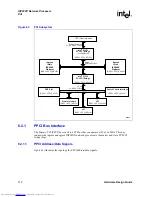
Table 39

 provides routing guidelines for the PPCI address/data group parameters.

6.2.1.2

PPCI Clock Signals

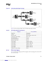
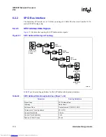
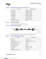
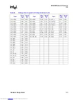
Figure 65

 illustrates the topology for PPCI clock signals. All of the clock signal traces for the PPCI 

bus should be matched.

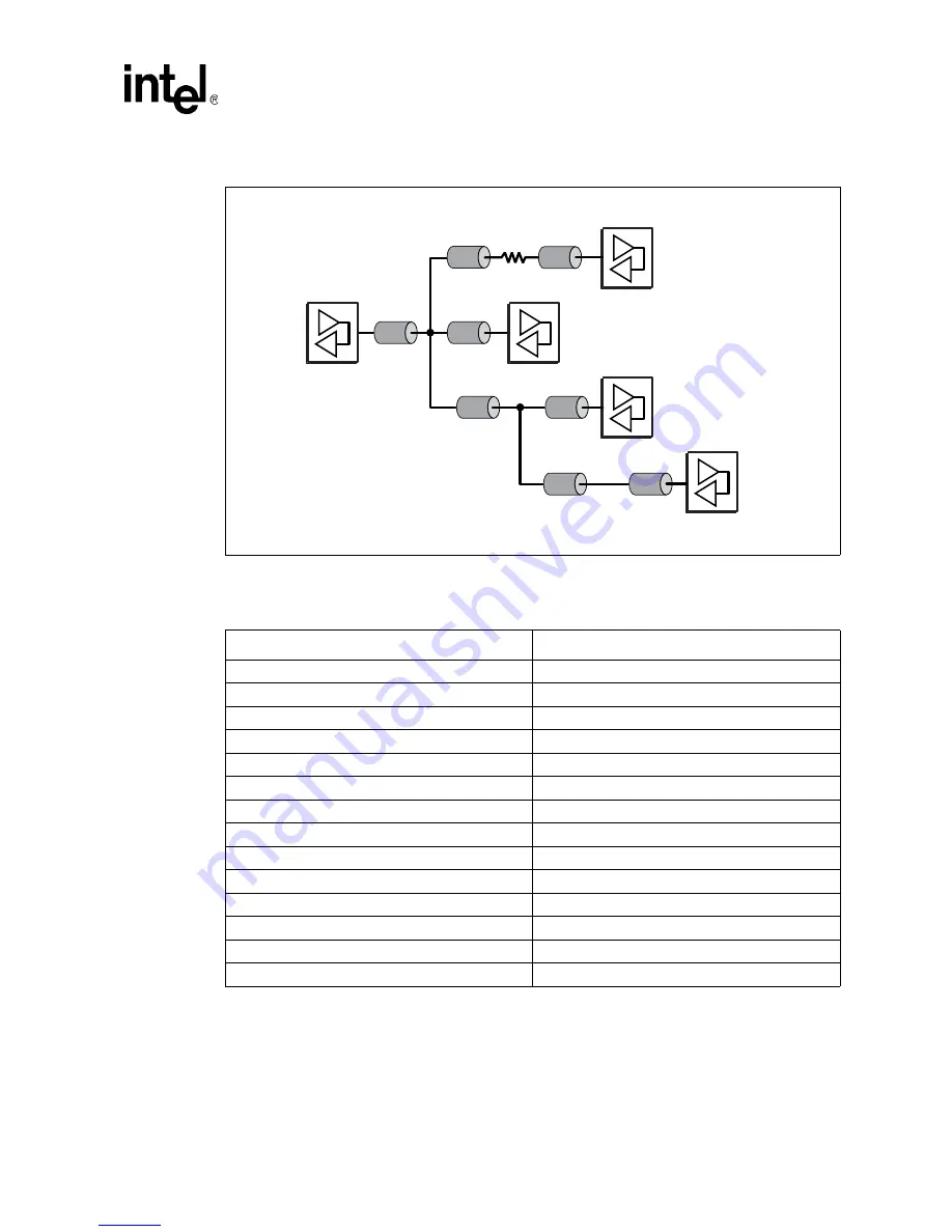
Figure 64. 

PPCI Address/Data Signal Topology


  !"


#


$

%

!

Table 39. 

PPCI Address/Data Group Guidelines

Parameter

Routing Guidelines

Signal Group

Address/Data

Topology

Daisy Chain

Reference Plane

Dual-referenced, PWR–SIG–GND

Characteristic Trace Impedance

60 

 ± 10%

Nominal Trace Width

3.5 mils

Nominal Trace Separation

9.0 mils

Spacing to Other Groups

20 mils

Trace Length A

Maximum = 50 mils

Trace Length B

Maximum = 4200 mils

Trace Length C

Maximum = 4500 mils

Trace Length D

Maximum = 50 mils

Trace Length E

Maximum = 1200 mils

Trace Length F

Maximum = 2500 mils

Maximum Via Count per Signal

8 Vias

Downloaded from 

Elcodis.com


electronic components distributor


Summary of Contents for IXP28 Series

Page 1: ...Order Number 309192 002US Intel IXP28XX Network Processors Hardware Design Guide August 2005 Downloaded from Elcodis com electronic components distributor ...

Page 2: ...ing life sustaining critical control or safety systems or in nuclear facility applications Intel may make changes to specifications and product descriptions at any time without notice Designers must not rely on the absence or characteristics of any features or instructions marked reserved or undefined Intel reserves these for future definition and shall have no responsibility whatsoever for confli...

Page 3: ... 2 5 2 Recommendations From Droop Analysis 31 3 RDRAM 33 3 1 IXMB2800 RDRAM Subsystem Design 33 3 1 1 RDRAM Subsystem Implementation Options 34 3 2 Rambus Channel Design 35 3 2 1 RSL Trace Requirements and Recommendations 35 3 2 2 Unused Channel Guidelines 36 3 2 3 Crosstalk 36 3 2 4 Third party Sources 36 3 2 5 IXP28XX Network Processor Power Up Sequence 36 3 2 6 IXP28XX Network Processor Power U...

Page 4: ... 1 Interface Topologies 81 4 8 IXDP2800 QDR Implementation Guidelines 84 4 8 1 Routing for a Four QDR SRAM Topology 84 4 8 2 Determining Loopclock Length for QDRII SRAM Used by IXDP2800 Advanced Development Platform 85 4 8 3 QDR SRAM Alternating Routing Layers 89 4 9 IXDP2800 TCAM Implementation 90 4 9 1 TCAM and QDR SRAM Placement 90 4 9 2 QDR SRAM and TCAM Routing Implementation 92 4 10 QDR SRAM...

Page 5: ...27 4 IXDP2800 Advanced Development Platform Power Supply Subsystem 28 5 IXDP2800 Advanced Development Platform Power up Sequence 29 6 IXP28XX Network Processor di dt Stimulus 30 7 Power up Sequence 37 8 Common VCCR_IO for All Three RACs in the IXP28XX Network Processor 38 9 Rambus Controller Footprint and Via Placement Showing Alternating Dogbone Orientation 39 10 Rambus Controller Footprint and V...

Page 6: ... Example for Each QDR Channel 81 45 Address D CONTROL Q and K Clocks Topologies 82 46 C C CIN and CIN Clocks Topologies 83 47 QDR SRAM Routing Recommendations 84 48 Four QDR SRAM Load Routing Recommendations 85 49 Example Interconnects on the IXP28XX Network Processor with a Two QDRII SRAM Load per Channel 86 50 Trace Length from IXP28XX Network Processor to SRAM C K SA D and R W_BW 87 51 Trace Le...

Page 7: ...IXP2850 Network Processor Package Marking 148 91 Intel IXP2800 or Intel IXP2850 Network Processor Package Ball Grid Array 149 92 Intel IXP2800 or Intel IXP2850 Network Processor Package Side View 149 93 Intel IXP2800 or Intel IXP2850 Network Processor Package Top View 150 Tables 1 Product Features of IXP28XX Network Processors 12 2 Guide Conventions 14 3 Acronyms and Terminology 14 4 Absolute Maxi...

Page 8: ...lines C C CIN and CIN Clocks 83 35 Package Trace Lengths for QDR Signals 96 36 Topology 1 Network Length Results 106 37 Topology 2 Network Length Results 107 38 Package Trace Lengths for LVDS_Diff Signals 108 39 PPCI Address Data Group Guidelines 113 40 PPCI Clock Signals Group Guidelines 114 41 Address Data Signal with IDSEL Group Guidelines 115 42 SPCI Address Data Group Guidelines 116 43 SPCI C...

Page 9: ...k Processor Revision History 9 Revision History Date Revision Description August 2005 002 Updates to Chapter 4 QDR SRAM December 2004 001 Initial release Downloaded from Elcodis com electronic components distributor ...

Page 10: ...IXP28XX Network Processor Revision History 10 Downloaded from Elcodis com electronic components distributor ...

Page 11: ...igures may display inconsistently For example viewing a figure on a computer screen and producing hardcopy to a printer can result in the screen providing finer resolution than the printer 1 1 System Overview The IXP28XX network processors enable fast deployment of complete content processing by providing unlimited programming flexibility code re use and high performance processing These network p...

Page 12: ...and 256 bit keys Three industry standard RDRAM interfaces Peak bandwidth of 2 1 Gbytes sec 800 MHz and 1066 MHz RDRAM Error Correction Code ECC Addressable from Intel XScale core Microengines and PCI Four industry standard 32 bit QDR SRAM interfaces Peak bandwidth of 1 9 Gbytes sec per channel 233 MHz SRAM Hardware support for Linked List and Ring operations Atomic bit operations Atomic arithmetic...

Page 13: ...I Local Bus Specification Version 2 2 interface for the IXP28XX network processor Chapter 7 Slowport describes the Slowport external interface to the IXP28XX network processor Chapter 8 Mechanical Packaging describes the dimensions of the IXP28XX network processor and package markings for the processor chip Figure 1 IXP2800 IXP2850 Network Processor Functional Block Diagram B0564 02 Media Switch F...

Page 14: ...oice of menu items For example the menu items for the Developers Workbench are Start IXA SDK 4 1 DevWorkbench Table 3 Acronyms and Terminology Sheet 1 of 3 Acronym Terminology Definition AES Advanced Encryption Standard ATM Asynchronous Transfer Mode BGA ball grid array BWE Byte Write Enable a type of control signal that is active low CFM Clock to Master positive polarity CFMN Clock to Master nega...

Page 15: ...m Access Memory RDRAM Rambus Dynamic Random Access Memory RIMM Rambus In line Memory Module used with RDRAM chips developed by Rambus Inc RPE Read Port Enable a type of control signal that is active low RSL Rambus Signaling Level SDH Synchronous Digital Hierarchy a set of international fiber optic transmission standards SF Switch Fabric SHA 1 Secure Hash Algorithm 1 SPCI Secondary PCI a 32 bit bus...

Page 16: ...tel IXP2800 Network Processor Electrical Mechanical and Thermal Specification EMTS Application Note Intel IXP2800 Network Processor IBIS Model Intel IXP2800 Network Processor BSDL File PCI Local Bus Specification Version 2 2 1 4 Contacting Intel TCAM Ternary Content Addressable Memory TM Traffic Manager UART Universal Asynchronous Receiver Transmitter VOQ Virtual output queue VRM Voltage Regulator...

Page 17: ...C Junction Temp Tj Extended 120 C Storage Temperature Range 55 C 125 C Supply Voltage Difference VDELTA 2 7 V 3 3 V to 2 5 V rail difference 3 3 V to 1 35 1 3 1 2 V rail difference VCORE 1 35 1 3 V Minimum Operating Voltage 1 1 V VCORE 1 2 V Minimum Operating Voltage 1 1 V Maximum power up time 700 ms It is expected that all supplies will be up and stable within 700 milliseconds Table 5 Functional...

Page 18: ...t over SONET POS reference design processing minimum size packets 49 bytes running at full OC 192 line rate Device2 2 Total power Typical Maximum Frequency IXP2800 Bn3 3 Bn refers to B0 and B1 25 5 W 31 5 W 1 4 GHz IXP2800 Bn 18 5 W 23 W 1 0 GHz IXP2800 Bn 12 5 W 16 W 650 MHz IXP2850 Bn 27 5 W 34 W 1 4 GHz IXP2850 Bn 20 5 W 25 W 1 0 GHz IXP2850 Bn 14 W 17 5 W 650 MHz Downloaded from Elcodis com el...

Page 19: ...3 V GND 5 N A 3 Clock PLL VCC_PLL VSS VCC_CLK VREFHI_CLK VREFLO_CLK PLL power PLL ground Ref Clock power also for GPIO Clock reference voltage Clock reference voltage 1 3 V GND 2 50 V 1 40 V 1 00 V 5 N A 5 5 5 1 3 SPI 4 CSIX F LOW VCC25V VCCA_FC VCCA_SPI4 VREFHI VREFLO SPI 4 supply also for PCI DLL power DLL power SPI 4 flow reference voltage SPI 4 flow reference voltage 2 50 V 1 3 V 1 3 V 1 40 V ...

Page 20: ... voltage SPI 4 flow reference voltage 2 50 V 1 2 V 1 2 V 1 40 V 1 00 V 5 5 5 5 5 1 1 3 3 GPIO VCC33 GPIO JTAG SP power 3 30 V 5 PCI VCC33_PCI PCI power supply 3 30 V 5 4 QDR VDDQ PAS0_VCCA PAS1_VCCA PAS2_VCCA PAS3_VCCA VREF_QDR0 VREF_QDR1 VREF_QDR2 VREF_QDR3 QRD power supply DLL power DLL power DLL power DLL power QDR reference voltage QDR reference voltage QDR reference voltage QDR reference volt...

Page 21: ...LL DLL VCC_PLL VCCA_FC VCCA_SPI4 PAS0_VCCA PAS1_VCCA PAS2_VCCA PAS3_VCCA 1 0 W 1 0 W Supplies 1 50 V VDDQ 2 0 W 2 0 W 1 80 V VCCRIO 0 5 W 0 5 W 2 5 V VCC_CLK VCC25V 1 8 W 1 8 W 3 3 V VCC33 VCC33_PCI 0 7 W 0 7 W 0 75 VREF_QDR0 VREF_QDR1 VREF_QDR2 VREF_QDR3 0 01 W 0 01 W Voltage References 1 0 V VREFLO_CLK VREF_LO 0 01 W 0 01 W 1 4 V VREFHI_CLK VREFHI PAR0_PADVREFA PAR0_PADVREFB PAR1_PADVREFA PAR1_P...

Page 22: ...L DLL VCC_PLL VCCA_FC VCCA_SPI4 PAS0_VCCA PAS1_VCCA PAS2_VCCA PAS3_VCCA 1 0 W 1 0 W Supplies 1 50 V VDDQ 2 0 W 2 0 W 1 80 V VCCRIO 0 5 W 0 5 W 2 5 V VCC_CLK VCC25V 1 8 W 1 8 W 3 3 V VCC33 VCC33_PCI 0 7 W 0 7 W 0 75 V VREF_QDR0 VREF_QDR1 VREF_QDR2 VREF_QDR3 0 01 W 0 01 W Voltage References 1 0 V VREFLO_CLK VREF_LO 0 01 W 0 01 W 1 4 V VREFHI_CLK VREFHI PAR0_PADVREFA PAR0_PADVREFB PAR1_PADVREFA PAR1_...

Page 23: ...L DLL VCC_PLL VCCA_FC VCCA_SPI4 PAS0_VCCA PAS1_VCCA PAS2_VCCA PAS3_VCCA 1 0 W 1 0 W Supplies 1 50 V VDDQ 1 9 W 1 9 W 1 80 V VCCRIO 0 4 W 0 4 W 2 5 V VCC_CLK VCC25V 1 7 W 1 7 W 3 3 V VCC33 VCC33_PCI 0 7 W 0 7 W 0 75 V VREF_QDR0 VREF_QDR1 VREF_QDR2 VREF_QDR3 0 01 W 0 01 W Voltage References 1 0 V VREFLO_CLK VREF_LO 0 01 W 0 01 W 1 4 V VREFHI_CLK VREFHI PAR0_PADVREFA PAR0_PADVREFB PAR1_PADVREFA PAR1_...

Page 24: ... or after the 2 5 V 1 3 V and 3 3 V supplies Note No 3 3 V devices should drive any of the IXP2800 IXP2850 pins until its 3 3 V supply is up and stable 2 2 2 Sequence for 650 MHz Devices The sequence for the 650 MHz B stepping devices is as follows 1 The 2 5 V supply must come up before the 1 2 V supply 2 The 1 2 V supply must come up after the 2 5 V supply and must not start to ramp until the 2 5...

Page 25: ...requency and bulk capacitors should be used to account for transient power steps The number and size of decoupling capacitors required for a particular implementation depends on the board stack up and power delivery circuitry so a single solution will not work for all implementations Note that the worst case transient occurs when the device comes out of reset as explained in Section 2 2 3 1 The IX...

Page 26: ...s for the IXP2800 or IXP2850 network processor For L1 a 10 Ω ferrite bead with a DCR of less than 0 1 Ω should be used For C1 a 10 µF capacitor should be used and each analog VCC pin should be decoupled with a 0 1 µF and a 0 01 µF capacitor The IXDP2800 Advanced Development Platform uses analog power for all PLL DL pins Figure 2 IXDP2800 Decoupling Implementation Downloaded from Elcodis com electr...

Page 27: ...bsystem is described with a block diagram and a power up sequence Section 2 4 1 Subsystem Block Diagram Section 2 4 2 Power up Sequence 2 4 1 Subsystem Block Diagram Figure 2 is a block diagram for the IXDP2800 Advanced Development Platform power supply subsystem Figure 3 LC Filter Network B0138 02 01 µF 0 1 µF 01 µF 0 1 µF 01 µF 0 1 µF L1 10 Ω 1 35V 1 3V 1 2V C1 10 µF Downloaded from Elcodis com ...

Page 28: ...ax 1 8V 2 Linear Intel IXP2800 Network Processor QDR RDRAM 16A max 0 75V Amps QDR Term 1A max Control Amps PMC and Control Amps 1 2V 1 Linear TCAM 6A max 2 5V 1 FET Intel IXP2800 Network Processor Logic I O 8A max 3 3V 1 FET Intel IXP2800 Network Processor Logic PCI 10A max 1 4V reference Intel IXP2800 Network Processor SPI Rambus 1 0V reference Intel IXP2800 Network Processor Clk SPI Chassis Moun...

Page 29: ...ower up sequence for the IXDP2800 Advanced Development Platform power supply Figure 5 IXDP2800 Advanced Development Platform Power up Sequence B3430 01 Time 150 ms 3 3 V 2 5 V 1 5 V 1 35 V 1 4 V 1 2 V 1 0 V 75 V 1 8 V Egress 1 8 V Ingress 300 ms 450 ms S U P P L Y Supply Downloaded from Elcodis com electronic components distributor ...

Page 30: ...p i e the transient step over 9 cycles at a 1 4 GHz clock rate 1540 A per µs at VDDMAX Power decreases by 13 21 W to 13 28 W approximately 67 REF_CLK cycles after PLL locks in one cycle Sensitivity analysis shows that a duration of tr2 see Figure 6 does not affect the first second or third droop Figure 6 IXP28XX Network Processor di dt Stimulus B3556 01 I B Step Power Up Condition 1 365 V with Mic...

Page 31: ...1 and tr2 transient events The Second Droop magnitude is 78 4 mV which occurs at 0 67 µs after transient The second droop depends on when the Microengines come out of reset specifically how much time this occurs after PLL locks and power starts decreasing The Third Droop magnitude is 67 6 mV which occurs between 10 1 13 1 µs after transient Assuming Voltage Regulator Bandwidth 10 KHz Cbulk is only...

Page 32: ...32 Hardware Design Guide IXP28XX Network Processor Power Ratings and Requirements Downloaded from Elcodis com electronic components distributor ...

Page 33: ...es Interleaving helps to maintain utilization of available bandwidth by spreading consecutive accesses to multiple channels The interleaving is done in the hardware so that the three channels appear to software as a single contiguous memory space ECC Error Correcting Code is supported but can be disabled Enabling ECC or parity requires that x18 RDRAMs be used if ECC is disabled x16 RDRAMs can be u...

Page 34: ... Option Memory per NPU Comments Using 256 Mbyte part Using 512 Mbyte part Short channel with two devices 192 Mbytes 384 Mbytes Clam shell configuration helps in layout Observability of clam shell components is an issue Must follow all design rules defined in the Rambus Short Channel Design Guide Short channel with four devices 384 Mbytes 768 Mbytes Clam shell configuration helps in layout Observab...

Page 35: ...ce the trace lengths provided in Section 3 7 must be adjusted to reflect the flight delay of the target PCB An example of this is provided in Section 3 7 For impedance control use the following guidelines 34 Ω for a short channel and 28 Ω for a long channel Trace widths for the desired impedance should be obtained from the manufacturer of the PCB as field solvers may not be accurate Device loading...

Page 36: ...nd floods are provided in the various Rambus layout guides Avoid routing over plane splits and voids 3 2 4 Third party Sources Detailed design and layout guides are available from Rambus for short channel RIMM and SO RIMM designs the information is not provided in this document since many third party vendors change information from time to time and could result in inconsistencies between the docum...

Page 37: ... 3 2 6 IXP28XX Network Processor Power Up Considerations when using NexMod Memory Modules The following are additional design considerations for the IXP28XX network processor s power up sequence when using NexMod modules Because each channel can have a separate power source for VTERM and VCMOS when using the HCD memory modules and VCCR_IO the RDRAM I O supply for the IXP28XX network processor is c...

Page 38: ...rate the IXP28XX network processor Rambus controller footprint and via placement Figure 9 Rambus Controller Footprint and Via Placement Showing Alternating Dogbone Orientation Figure 10 Rambus Controller Footprint and Via Placement Showing Exploded View of Checkerboard Detail Figure 9 illustrates the IXP28XX network processor Rambus controller footprint and via placement The checkerboard GND signa...

Page 39: ...re Design Guide 39 IXP28XX Network Processor RDRAM Figure 9 Rambus Controller Footprint and Via Placement Showing Alternating Dogbone Orientation Downloaded from Elcodis com electronic components distributor ...

Page 40: ... IXP28XX network processor Rambus controller footprint and via placement showing an exploded view of checkerboard detail Figure 10 Rambus Controller Footprint and Via Placement Showing Exploded View of Checkerboard Detail Downloaded from Elcodis com electronic components distributor ...

Page 41: ... Processor Controller Escape Routing Layer 6 Figure 13 Network Processor Controller Escape Routing Layer 13 Figure 14 Network Processor Controller Escape Routing SCK CMD Signals Routed on Layer 12 Figure 15 Network Processor Controller Escape Routing SCK CMD Signals Routed on Layer 16 Figure 11 illustrates layer 4 of the IXP28XX network processor controller escape routing using 28 Ω 11 mil wide tr...

Page 42: ...r RDRAM Figure 12 illustrates layer 6 of the IXP28XX network processor controller escape routing using 28 Ω 11 mil wide traces Figure 12 Network Processor Controller Escape Routing Layer 6 Downloaded from Elcodis com electronic components distributor ...

Page 43: ... RDRAM Figure 13 illustrates layer 13 of the IXP28XX network processor controller escape routing using 28 Ω 11 mil wide traces Figure 13 Network Processor Controller Escape Routing Layer 13 Downloaded from Elcodis com electronic components distributor ...

Page 44: ...strates IXP28XX network processor controller escape routing on layer 12 with SCK CMD signals using 28 Ω 11 mil wide traces Figure 14 Network Processor Controller Escape Routing SCK CMD Signals Routed on Layer 12 Downloaded from Elcodis com electronic components distributor ...

Page 45: ...strates IXP28XX network processor controller escape routing on layer 16 with SCK CMD signals using 28 Ω 11 mil wide traces Figure 15 Network Processor Controller Escape Routing SCK CMD Signals Routed on Layer 16 Downloaded from Elcodis com electronic components distributor ...

Page 46: ...lemented on the IXMB2800 development system Figure 16 Three Channel Controller to HCD NexMod RDRAM Routing Layer 4 Figure 17 Three Channel Controller to HCD NexMod RDRAM Routing Layer 6 Figure 18 Three Channel Controller to HCD NexMod RDRAM Routing Layer 13 Figure 19 Three Channel Controller to HCD NexMod RDRAM Routing SCK CMD Layer 12 Figure 16 Three Channel Controller to HCD NexMod RDRAM Routing...

Page 47: ...Hardware Design Guide 47 IXP28XX Network Processor RDRAM Figure 17 Three Channel Controller to HCD NexMod RDRAM Routing Layer 6 Downloaded from Elcodis com electronic components distributor ...

Page 48: ...etwork Processor RDRAM Figure 18 Three Channel Controller to HCD NexMod RDRAM Routing Layer 13 Figure 19 Three Channel Controller to HCD NexMod RDRAM Routing SCK CMD Layer 12 Downloaded from Elcodis com electronic components distributor ...
Page 49: ...P28XX network processor short channel routing example Note The layout example depicted in Figure 20 was implemented only as a routing study and has not been validated Figure 20 IXP28XX Network Processor Short Channel Routing Terminations RDRAMs Intel IXP28XX Network Processor Downloaded from Elcodis com electronic components distributor ...
Page 50: ... 12 549 0 494 RDR2_DQA 8 18 573 0 731 RDR0_RQ 3 16 938 0 667 RDR1_CMD 12 436 0 490 RDR2_CTM 18 264 0 719 RDR0_DQB 2 16 78 0 661 RDR1_DQA 6 11 982 0 472 RDR2_CTMN 18 264 0 719 RDR0_RQ 0 16 517 0 650 RDR1_DQA 0 11 567 0 455 RDR2_DQA 6 17 226 0 678 RDR0_DQB 6 15 93 0 627 RDR1_DQB 8 11 316 0 446 RDR2_DQA 4 16 687 0 657 RDR0_RQ 5 15 727 0 619 RDR1_DQB 7 11 167 0 440 RDR2_DQA 1 16 358 0 644 RDR0_SIO 15 ...

Page 51: ...DR1_DQB 3 7 565 0 298 RDR2_SCK 10 513 0 414 RDR0_DQA 7 9 961 0 392 RDR1_DQA 3 7 273 0 286 RDR2_PCLKM 10 254 0 404 RDR0_DQA 0 8 655 0 341 RDR1_DQB 0 6 813 0 268 RDR2_DQB 5 9 806 0 386 RDR0_DQA 8 8 306 0 327 RDR1_SIO 6 608 0 260 RDR2_SCLKN 9 157 0 361 RDR0_DQA 3 8 001 0 315 RDR1_RQ 4 6 421 0 253 RDR2_CMD 8 958 0 353 Table 13 Package Trace Lengths for RDRAM Signals Sheet 2 of 2 Signal Metric Units mm...

Page 52: ...52 Hardware Design Guide IXP28XX Network Processor RDRAM Downloaded from Elcodis com electronic components distributor ...

Page 53: ...essor The network processor supports bursts of two SRAMs four SRAM bursts are not supported The SRAM controller can also be configured to interface to an external coprocessor that adheres to the QDR electricals and protocol Each SRAM controller can also interface to an external coprocessor through its standard QDR interface which enables SRAM devices and coprocessors to operate on the same bus The...

Page 54: ...h address pins 24 to support up to 64 Mbytes of SRAM The SRAM controllers can directly generate multiple port enables up to four pairs to allow for depth expansion two pairs of pins are dedicated for port enables Smaller RAMs use fewer address signals than the number provided to accommodate the largest RAMs so some address pins 23 20 are configurable as either address or port enable based on the c...

Page 55: ... 20 4 2M x 18 4 Mbytes 19 0 23 22 21 20 4 4M x 18 8 Mbytes 20 0 23 22 3 8M x 18 16 Mbytes 21 0 23 22 3 16M x 18 32 Mbytes 22 0 None 2 32M x 18 64 Mbytes 23 0 None 1 Table 15 QDR Address RPE WPE Mapping SRAM Configuration Size SRAM_CONTROL SRAM_SIZE 9 7 SRAM_CONTROL PORT_CTL 5 4 RPE 2 WPE 2 RPE 3 WPE 3 512K x 18 1 Mbyte 000 11 QDR_ADDR 23 22 QDR_ADDR 21 20 1Mb x 18 2 Mbytes 001 11 QDR_ADDR 23 22 QD...

Page 56: ...ytes 48 Mbytes 64 Mbytes NA NA NA NA 16M x 18 32 Mbytes 64 Mbytes NA NA NA NA NA NA 32M x 18 64 Mbytes NA NA NA NA NA NA NA Table 16 Total Memory per Channel Sheet 2 of 2 SRAM Size Number of SRAMs on Channel 1 2 3 4 5 6 7 8 Downloaded from Elcodis com electronic components distributor ...

Page 57: ...cement for the pipelined QDR SRAM a coprocessor with QDR signaling capability Figure 22 QDR SRAM Connections B3414 01 C C 0 K K 0 Q 17 0 D 17 0 D 17 0 Q 17 0 SA 21 0 ZQ SA 21 0 BW 1 0 BW 1 0 W R W 0 R 0 W R 1 ZQ 0 ZQ 1 CIN CIN 0 C C 1 K K 1 CIN CIN 1 C C K K CQ CQ D 17 0 Q 17 0 ZQ SA 21 0 BW 1 0 NW 1 0 NW 1 0 W R C C K K CQ CQ 250 Ohms 250 Ohms 50 Ohms 50 Ohms 0 Ohms 1 5 V Not Used Not Used Intel ...

Page 58: ...cal loads can be achieved on one side of the PCB however it is recommended that simulation first verify that timing meets the specification and that signal integrity is maintained With a two SRAM load topology the DATA READ cycle s signal integrity issue is less serious than in the four SRAM load because there is only one stub hanging on the net The more stubs the net has the more serious and seve...

Page 59: ...cating two devices on opposite sides of the PCB is possible with either width expansion or depth expansion Figure 23 Topologies for Using x9 Versus x18 QDR SRAM Parts B3950 01 Stub Stub Top SRAM READ Topology Using Two x9 SRAM Parts Half DATA Bus 9 bits wide B Intel IXP2800 Receiver Bottom SRAM Stub Stub Top SRAM Bottom SRAM Half DATA Bus 9 bits wide B Intel IXP2800 Receiver On die Termination 50 ...

Page 60: ...00 Width Expanded QDR Interface Figure 25 Ingress IXP28XX Network Processor QDR Modular Channel Depth Expanded QDR Interface Figure 26 Ingress IXP2800 Network Processor QDR Modular Channel Four Load QDR Interface Figure 24 IXP2800 Width Expanded QDR Interface1 1 On egress channels 1 and 2 and ingress channel 1 9 9 Downloaded from Elcodis com electronic components distributor ...
Page 61: ...R SRAM Figure 25 Ingress IXP28XX Network Processor QDR Modular Channel Depth Expanded QDR Interface Figure 26 Ingress IXP2800 Network Processor QDR Modular Channel Four Load QDR Interface 9 9 9 Downloaded from Elcodis com electronic components distributor ...
Page 62: ...35 Ohm Center T Point K Clocks Point to Point 50 Ohm Driver 50 Ohm 2 SRAMs 50 Ohm SRAM Input C Clocks Point to Point 50 Ohm Driver 50 Ohm 2 SRAMs 50 Ohm On Die IXP2800 CIN Inputs D Write T Topology Daisy Chain 50 Ohm Driver 50 Ohm 2 SRAMs 50 Ohm T Point Q Read T Topology SRAM 50 Ohm 2 SRAMs 50 Ohm On Die IXP2800 Control WPE RPE T Topology 30 Ohm Driver 34 Ohm 2 SRAMs 35 Ohm T Point Control BWE T T...

Page 63: ..._H 8 Q 8 Q 8 On die at IXP28XX Receiver QDRn_D_H 16 9 D 7 0 D 7 0 PU50Ω QDRn_D_H 17 D 8 D 8 PU50Ω QDRn_D_H 7 0 D 7 0 D 7 0 PU50Ω QDRn_D_H 8 D 8 D 8 PU50Ω QDRn_RPS_L 0 R R PU35Ω Center Termination at T junction QDRn_WPS_L 0 W W PU35Ω Center Termination at T junction QDRn_RPS_L 1 R R PU35Ω Center Termination at T junction QDRn_WPS_L 0 W W PU35Ω QDRn_BWS_L 0 BW BW PU35Ω QDRn_BWS_L 1 BW BW PU35Ω VDDQ ...

Page 64: ...for this operation for the driver side QDR SRAM is described in the specification sheet of the SRAM provided by the SRAM manufacturer For further information about IXP2800 input timing refer to the Intel IXP2800 and IXP2850 Network Processors Datasheet 4 4 5 2 IXP2800 Output Timing The IXP28XX network processor output timings provide for the output timing requirements of the network processor s dr...

Page 65: ... must be length matched together the Data OUT nets must be matched together and so on However the length of a Data OUT net for example needs does not need to be matched to an Address net etc A complete listing of package trace lengths for all nets in all groups would be available in a separate spreadsheet This spreadsheet can be used to do the length matching of the nets The following are QDR trac...

Page 66: ...topology for QDR address signals Table 19 provides routing guidelines for the QDR address signal group Figure 27 QDR Address Signals Balanced T Topology 9 Figure 28 QDR Address Routing T Topology with Daisy Chain Branches 9 Downloaded from Elcodis com electronic components distributor ...
Page 67: ... length Should be matched to K Clk trace length minus 0 9 inches Maximum 11 0 inches Trace length from ball to ball for all Address nets should be matched for the entire group to within 25 mils Trace length B C As short as possible B and C should match Maximum B E 1 0 inches Maximum C F 1 0 inches Trace length D As short as possible Maximum 100 mils Trace length E F As short as possible Maximum B ...

Page 68: ...d signals Therefore for Data OUT signals a daisy chain configuration would be used for its topology A better choice however is to use a T topology for Data OUT whenever it is possible Figure 30 illustrates the routing topology for QDR SRAM D Data Out Table 21 provides routing guidelines for the QDR D signal group Table 20 QDR Address Stack up Signal Cross section Details Parameter QDR Signal Trace...

Page 69: ...inches Trace length B As short as possible Maximum 0 4 inches Trace length C Maximum 0 5 inches Trace length D As short as possible Maximum 1 0 inch Maximum via count per signal As small as possible Maximum 7 vias Length tuning method All D signals matched within 25 mils where length includes package length compensation P A Figure 31 QDR D Signal Trace Width Spacing Routing B3992 01 20 mil or larg...

Page 70: ... Die Termination QDR Top SRAM QDR Bottom SRAM T Topology Data In Q0 Q7 Q9 Q16 Parity In Q8 Q17 Signals Table 23 QDR Q Data In Signal Group Routing Guidelines Parameter Routing Guideline Signal Group Q Topology Matched T topology Reference Plane Ground Characteristic Trace Impedance 50 Ω 10 RTT 50 Ω 1 on die termination at the IXP28XX receiver Nominal Trace Width 5 mils Nominal Trace Separation 8 1...

Page 71: ...als are mirrored in the SRAM part Thus the topology of choice for the K Clocks is a point to point topology with two SRAMs clam shelled Figure 34 illustrates the routing topology for QDR K and K 1 P refers to the package length Figure 33 QDR Q Signal Trace Width Spacing Routing B3992 01 20 mil or larger Prepreg S W W Other Signals POWER or GND Plane POWER or GND Plane Td2 Td1 Tsignal DATA Signal D...

Page 72: ...Ω 10 RTT 50 Ω 1 Nominal Trace Width 5 mils Nominal Trace Separation 20 mils Group spacing Isolation from all other signals is 20 25 mils Trace length P1 A to SRAMs 1 P refers to the package length Trace length from ball to ball should be within 25 mils for all K K nets Trace length B As short as possible Maximum 1 0 inches Maximum via count per signal As short as possible Maximum 6 vias Length tun...

Page 73: ...he Data OUT CONTROL and Address at the same time Therefore it becomes necessary to match their flight times with respect to each other Matching their flight times means adjusting their trace lengths with respect to each accordingly If the trace length of on of these three signals is fixed the individual trace length of each one of the other signals must be controlled according to the following K C...

Page 74: ...d output data Ideally C is 180 degrees out of phase with C Figure 36 illustrates the routing topology for QDR C C CIN and CIN Table 27 provides routing guidelines for the QDR C C CIN and CIN signal groups Figure 36 QDR C C CIN and CIN Routing Topology B3957 01 A Intel IXP2800 Driver Cout Clock C C C Clk signal C C and CIN CIN Top SRAM Bottom SRAM B Intel IXP2800 Receiver Cin Clock CIN CIN On Die T...

Page 75: ...h Pkg1 A to SRAMs Roughly matched to B Maximum 11 0 inches Trace length B Should be matched to Q trace length Maximum 11 0 inches Maximum via count per signal As small as possible Maximum 6 vias Length tuning method All C and C signals should be length matched among each other to within 25 mils Table 27 QDR C C CIN and CIN Signal Group Routing Guidelines Sheet 2 of 2 Parameter Routing Guideline Fi...

Page 76: ...dance and trace spacing would be the same as in the Address Only the trace length would be different and similar to the Data OUT for flight time matching purposes Alternatively these signals can be treated as the Data OUT signals due to their similarity in the number of loads In this case the driver buffer strength the termination resistance the trace impedance and the trace spacing and trace leng...

Page 77: ...ch Maximum via count per signal As small as possible Maximum 7 vias Length tuning method All CONTROL signals matched within 25 mils where length includes package length compensation P A 1 P refers to the package length Table 29 QDR Control RPE and WPE Signal Group Routing Guidelines Sheet 2 of 2 Parameter Routing Guideline Figure 39 QDR Control RPE and WPE Signal Trace Width Spacing Routing POWER ...

Page 78: ...33 Ω 10 RTT 35 Ω 1 Nominal Trace Width 5 mils Nominal Trace Separation 15 mils or more Group Spacing Isolation from all other signals is 20 25mils Trace length P1 A to SRAMs 1 P refers to the package length Should be matched to K Clk trace length minus 0 5 inches Maximum 11 0 inches Trace length B As short as possible Maximum 0 4 inches Trace length C Maximum 0 5 inches Trace length D As short as ...

Page 79: ...er which is then fed through an optical amplifier to create a noise sensitive voltage reference Figure 43 and Figure 44 show a resistor divider circuit to generate the VREF supply Figure 41 Control BWE Signal Trace Width Spacing Routing POWER or GND Plane POWER or GND Plane Table 32 QDR CONTROL Stack up Signal Cross section Details Parameter QDR Signal Trace Width W mils Trace Thickness Tsignal mi...

Page 80: ...stive voltage divider should be used for each QDR SRAM channel Figure 44 shows an example of a voltage QDR VREF divider for each QDR channel Figure 42 QDR SRAM VREF Generation Figure 43 Resistive QDR VREF Divider Example Downloaded from Elcodis com electronic components distributor ...
Page 81: ...rt for up to four QDRII SRAMs 4 7 1 TCAM SRAM Coprocessor Interface Base Card Side This part of the interface runs between the ingress IXP28XX network processor and the Mictor connector on the base card side All traces are matched in length to within 10 mils and have the same nominal line impedance of 50 Ω 4 7 1 1 Interface Topologies This part of the interface has a topology of a point to point c...

Page 82: ...able 33 TCAM SRAM Coprocessor Interface Guidelines Address D CONTROL Q and K Clocks Parameter Routing Guideline Signal Group TCAM SRAM coprocessor Address D CONTROL Q and K Clocks Topology Point to Point Reference Plane Ground Characteristic Trace Impedance 50 Ω 5 Nominal Trace Width 5 mils Nominal Trace Separation for group 8 to 15 mils Group spacing Isolation from non QDR and non group related s...

Page 83: ...cks Parameter Routing Guideline Signal Group TCAM SRAM coprocessor C C CIN and CIN Clocks Topology Point to Point Reference Plane Ground Characteristic Trace Impedance 50 Ω 5 Nominal Trace Width 5 mils Nominal Trace Separation for group 8 to 15 mils Group spacing Isolation from non QDR and non group related signals is 20 mils IXP28XX breakout guideline 3 5 mils with 4 mil space for a maximum of 40...

Page 84: ...frequency is effectively approximately 167 MHz The following are routing recommendations for four QDR SRAM topologies Only terminate lines on IXP28XX network processor drives OUTCLK OUTCLK_L is 4 5 inches The x9 devices are recommended for topologies that use four loads and for 200 MHz operations The x18 devices are recommended for 167 MHz operations Figure 47 QDR SRAM Routing Recommendations B341...

Page 85: ...t is reduced and board layout is simplified Using one clock pair C_H 0 C_L 0 K_H 0 K_L 0 from the IXP28XX network processor to drive the SRAM devices and the other pair C_H 1 C_L 1 to clock the Q data back into the IXP28XX network processor provides the widest timing margin Each clock is effectively point to point reducing the load of each clock and decreasing uncertainty Figure 48 Four QDR SRAM L...

Page 86: ...r to SRAM C K SA D and R W_BW Figure 51 illustrates the trace length from SRAM to the IXP28XX network processor Q data Figure 49 Example Interconnects on the IXP28XX Network Processor with a Two QDRII SRAM Load per Channel Intel IXP2800 QDR Channel QDR II SRAM QDR II SRAM Downloaded from Elcodis com electronic components distributor ...
Page 87: ...ident with the rising edge of Q data i e the loopback clock should arrive at the network processor die at the same time as the Q data even though they follow different paths In the case of the loopback clock only the C clock length from the IXP28XX network processor to SRAM and the Q data length from SRAM to the network processor need to be considered It is assumed that the total C and C_N etch le...

Page 88: ... Delta term Since C 0 and Q lines have more capacitance loading than C 1 loopclock C 0 and Q slew rates are slower with respect to C 1 The capacitance per pin for a Micron QDRII SRAM is 5 pF minimum to 6 pF maximum and the capacitance for an IXP28XX network processor input pin is 5 pF minimum to 10 pF maximum Therefore the total capacitive load at the end of the line on C 0 is two SRAMs for 10 pF ...

Page 89: ...r adjacent QDR clamshell pairs as implemented on the IXDP2800 Advanced Development Platform Figure 52 QDR 0 Routing on Layer 13 Adjacent QDR Clamshell Pairs Figure 53 QDR 1 Routing on Layer 12 Adjacent QDR Clamshell Pairs Figure 52 QDR 0 Routing on Layer 13 Adjacent QDR Clamshell Pairs QDR 0 routing on layer 13 Downloaded from Elcodis com electronic components distributor ...
Page 90: ...cribes the placement and routing implementation for the TCAM and QDR SRAM 4 9 1 TCAM and QDR SRAM Placement Figure 54 illustrates TCAM and QDR SRAM placement Figure 53 QDR 1 Routing on Layer 12 Adjacent QDR Clamshell Pairs QDR 1 routing on layer 12 Downloaded from Elcodis com electronic components distributor ...

Page 91: ... 18 17 16 15 14 13 12 11 10 9 8 7 6 5 4 3 2 1 A B C D E F G H J K L M N P R T U V W Y AA AB AC AD AE AF AG AH AJ AK AL AM AN A B C D E F G H J K L M N P R T U V W Y AA AB AC AD AE AF AG AH AJ AK AL AM AN QDR SRAM Footprints Center of routing T TCAM footprint same power pin ball out as QDR SRAM Downloaded from Elcodis com electronic components distributor ...

Page 92: ...erminate lines on IXP28XX network processor drives OUTCLK OUTCLK_L is 4 4 5 inches 250 MHz performance Figure 55 Routing Recommendations for QDR SRAM and TCAM Routing B3424 01 Loopback Clock Length 7 5 1 5 2 0 0 75 1 0 L1 0 75 1 0 L2 0 25 0 75V 100 Ohms Intel IXP2800 Network Processor QDR SRAM QDR SRAM or TCAM L1 MUST EQUAL L2 0 25 0 75V 100 Ohms Downloaded from Elcodis com electronic components d...

Page 93: ...Figure 56 QDR Signal from IXP28XX Network Processor to Tee Point on Layer 12 Figure 57 QDR Signal Tee Point Arms Routed on Signal Layers 4 and 13 Figure 56 QDR Signal from IXP28XX Network Processor to Tee Point on Layer 12 QDR signal from IXP28XX Network Processor to Tee Point on layer 12 Downloaded from Elcodis com electronic components distributor ...

Page 94: ...rocessor but 1 5 V on QDR devices i e a level shift is necessary The IXP28XX network processor CIN 1 pins are NC from the I O pad to the SRAM controller internally Only CIN 0 is used to derive the read capture clock The CIN 1 pin can be used to terminate the clock and this I O pad is controllable via the RCOMP registers Refer to the Intel IXP2400 and IXP2800 Network Processor Programmer s Referenc...

Page 95: ... the difference in flight delay between the package and the PCB For example QDR0_Q_H 16 has a package length of 0 628 in and the target PCB has a flight delay of 180ps in In order to adjust the package length to match the PCB flight delay this length must be multiplied by the ratio of 154 180 or the difference between the package and PCB flight delays Therefore the trace package routing length tha...

Page 96: ...914 0 469 QDR1_CIN_H 1 10 0 394 QDR2_Q_H 3 12 564 0 495 QDR0_Q_H 1 11 594 0 456 QDR1_CIN_L 0 10 0 394 QDR2_Q_H 0 12 485 0 492 QDR0_C_H 0 11 5 0 453 QDR1_CIN_L 1 10 0 394 QDR2_Q_H 1 11 56 0 455 QDR0_C_L 0 11 5 0 453 QDR1_Q_H 1 8 684 0 342 QDR2_C_H 0 11 1 0 437 QDR0_Q_H 17 11 359 0 447 QDR1_Q_H 15 8 362 0 329 QDR2_C_L 0 11 1 0 437 QDR0_Q_H 0 10 095 0 397 QDR1_Q_H 13 7 899 0 311 QDR2_Q_H 15 9 226 0 3...

Page 97: ...92 0 236 QDR3_C_L 1 10 0 394 QDR0_D_H 4 10 73 0 422 QDR0_D_H 9 5 991 0 236 QDR3_Q_H 12 9 758 0 384 QDR0_D_H 13 10 495 0 413 QDR0_K_H 0 1 85 0 073 QDR3_Q_H 11 9 718 0 383 QDR0_A_H 21 10 105 0 398 QDR0_K_L 0 1 85 0 073 QDR3_Q_H 7 8 695 0 342 QDR0_A_H 22 9 924 0 391 QDR3_Q_H 14 8 056 0 317 QDR0_A_H 6 9 863 0 388 QDR3_Q_H 15 7 971 0 314 QDR0_A_H 13 9 798 0 386 QDR3_Q_H 17 7 617 0 300 QDR0_A_H 16 9 728...

Page 98: ...QDR2_D_H 11 7 213 0 284 QDR1_A_H 22 11 256 0 443 QDR2_K_L 1 16 0 630 QDR2_BWS_L 0 6 842 0 269 QDR1_A_H 3 11 256 0 443 QDR2_D_H 17 15 997 0 630 QDR2_D_H 8 6 781 0 267 QDR1_A_H 6 11 256 0 443 QDR2_D_H 15 15 403 0 606 QDR2_A_H 14 6 485 0 255 QDR1_A_H 7 11 256 0 443 QDR2_A_H 17 15 149 0 596 QDR2_A_H 19 6 479 0 255 QDR1_A_H 8 11 256 0 443 QDR2_D_H 1 14 881 0 586 QDR2_A_H 18 6 477 0 255 QDR1_BWS_L 1 11 ...

Page 99: ...13 6 0 236 QDR3_D_H 13 11 307 0 445 QDR3_A_H 8 6 0 236 QDR3_A_H 10 11 28 0 444 QDR3_A_H 11 5 996 0 236 QDR3_A_H 22 11 264 0 443 QDR3_D_H 2 5 981 0 235 QDR3_D_H 12 11 137 0 438 QDR3_A_H 6 10 963 0 432 QDR3_A_H 1 10 703 0 421 QDR3_A_H 4 10 654 0 419 QDR3_BWS_L 1 10 4 0 409 QDR3_A_H 15 10 328 0 407 QDR3_A_H 17 10 067 0 396 QDR3_D_H 4 9 077 0 357 QDR3_D_H 5 8 933 0 352 QDR3_D_H 7 8 916 0 351 QDR3_D_H ...

Page 100: ...100 Hardware Design Guide IXP28XX Network Processor QDR SRAM Downloaded from Elcodis com electronic components distributor ...
Page 101: ...ons The SPI 4 2 protocol transfers data in bursts of variable length Associated with each burst is information such as port number for a multi port device such as a 10 x 1 GbE SOP and EOP This information is collected by the MSF and passed to the Microengines The following implementations do not require an extra oscillator to provide a clock for the data that moves between two network processors o...

Page 102: ...g to CFrame category guaranteeing that neither control nor data CFrames block each other There are two types of CSIX L1 flow control Link Level Virtual Output Queue VOQ Every CFrame Base Header contains a Ready Field which contains two Link Level flow control bits one for Flow Control traffic and one for Data traffic Due to the CSIX L1 requirement for bounded response to Link Level flow control th...

Page 103: ...w Control Bus to the ingress IXP28SS network processor Additionally the egress IXP2800 or IXP2850 network processor sends incoming and outgoing Link Level flow control information across the Flow Control Serial Bus to the ingress IXP28XX network processor When the IXP2800 or IXP2850 network processor is configured in Simplex Mode the Flow Control Bus signals are connected directly to the Switch Fa...

Page 104: ... was routed with a minimum 4 mil trace width and a 10 mil trace pitch 6 mil spacing between lines these characteristics provide a 50 Ω trace and a 92 Ω differential impedance Routing the differential pair with a 4 mil trace width and a 15 mil trace pitch between signal pairs 11 mil spacing between lines yields a better impedance match at the expense of routing density 5 2 3 Design Review Checklist...

Page 105: ...ion guide above Termination rules are also discussed in detail in the MSF pin description section of the Intel IXP2800 and Intel IXP2850 Network Processors Datasheet 5 2 4 LVDS Routing Example Figure 60 illustrates LVDS routing as signal pairs with 15 mil trace spacing and an 11 mil air gap This stackup yields a 92 ohm differential impedance Note that the characteristic impedance is a function of ...

Page 106: ...igure 61 Figure 62 illustrates the connections between the IXP28XX network processor and an LVDS load device showing two unique connected PCBs with a loopback signal and connectors in each path Figure 61 Topology 1 Two Unique PCBs Connected B3404 01 LVDS Load Device Topology 1 Two unique PCBs connected via a connector Intel IXP2800 Network Processor L1 L2 Connector Table 36 Topology 1 Network Leng...

Page 107: ...ack Through Connectors B3405 01 L3 Intel IXP2800 Network Processor L1 TX RX L2 Connector Connector Topology 2 Two unique PCBs and the signal loops from PCB1 to PCB2 back to PCB1 with a connector in each path Table 37 Topology 2 Network Length Results Transfer Net L1 inches L2 inches L3 inches Maximum Total Etch Length inches EYE Opening mV FLOW_CONTROL 3 to 7 0 4 3 to 7 14 4 200 FLOW_CONTROL_CLK 3...

Page 108: ... in FC_RXCSRB_L 15 168 0 597 SPI4_TDAT 15 11 51 0 453 SPI4_TDAT 2 8 628 0 340 FC_RXCSRB 15 167 0 597 SPI4_RDAT 2 11 313 0 445 SPI4_TDAT_L 2 8 623 0 339 SPI4_RDAT 0 14 548 0 573 SPI4_RDAT_L 2 11 312 0 445 FC_RXCDAT_L 3 8 424 0 332 SPI4_RDAT_L 0 14 546 0 573 SPI4_RDAT_L 10 11 166 0 440 FC_RXCDAT 3 8 42 0 331 FC_RXCSOF_L 14 46 0 569 SPI4_RDAT 10 11 164 0 440 SPI4_TDAT 14 7 807 0 307 FC_RXCSOF 14 455 ...

Page 109: ...0 6 205 0 244 SPI4_RDAT_L 15 11 863 0 467 FC_TXCSOF 8 904 0 351 FC_TXCDAT_L 0 6 202 0 244 SPI4_TDAT_L 15 11 513 0 453 FC_TXCSOF_L 8 903 0 351 SPI4_TDAT 12 6 129 0 241 SPI4_TDAT_L 12 6 129 0 241 SPI4_RDAT 12 6 124 0 241 SPI4_RDAT_L 12 6 119 0 241 FC_TXCDAT_L 1 6 079 0 239 FC_TXCDAT 1 6 077 0 239 SPI4_TDAT_L 7 6 046 0 238 SPI4_TDAT 7 6 041 0 238 SPI4_TDAT 9 6 034 0 238 SPI4_TDAT_L 9 6 034 0 238 SPI4...

Page 110: ...110 Hardware Design Guide IXP28XX Network Processor MSF SPI 4 CSIX FC Downloaded from Elcodis com electronic components distributor ...

Page 111: ...ntroller with its own bus arbiter supporting two external masters in addition to the PCI unit s initiator interface The base card implementation requires more than two external masters therefore the arbiter in both the ingress and egress INXP2800 network processor is disabled and the arbiter in the 21555 PCI PCI bridge is enabled instead In this implementation both the ingress and egress network p...

Page 112: ...address data signals Figure 63 PCI Subsystem B3928 Primary 32 64 bit 33 66 MHz PCI Bus 64 bit 66 MHz PCI Bus 32 bit 33 MHz PCI Bus Ingress Intel IXP28XX Platform IDSEL PPCI_AD 21 Egress Intel IXP28XX Platform IDSEL PPCI_AD 23 Intel 21555 PCI PCI Bridge Config Master IDSEL PPCI_AD 22 PMC Slot IDSEL SPCI_AD 23 Media Interface IDSEL SPCI_AD 21 Switch Fabric Interface IDSEL SPCI_AD 22 Intel 21154 PCI ...

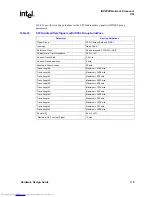
Page 113: ...roup Guidelines Parameter Routing Guidelines Signal Group Address Data Topology Daisy Chain Reference Plane Dual referenced PWR SIG GND Characteristic Trace Impedance 60 Ω 10 Nominal Trace Width 3 5 mils Nominal Trace Separation 9 0 mils Spacing to Other Groups 20 mils Trace Length A Maximum 50 mils Trace Length B Maximum 4200 mils Trace Length C Maximum 4500 mils Trace Length D Maximum 50 mils Tr...

Page 114: ...s Topology B0515 01 B PPCI Device A CLK Driver CY2305 RS Table 40 PPCI Clock Signals Group Guidelines Parameter Routing Guidelines Signal Group Clock Topology Point to Point Reference Plane Dual referenced PWR SIG GND Characteristic Trace Impedance 60 Ω 10 Nominal Trace Width 3 5 mils Nominal Trace Separation 9 mils Spacing to Other Groups 20 mils Trace Length A Maximum 200 mils Trace Length B Max...

Page 115: ...SEL Topology Daisy Chain Reference Plane Dual referenced PWR SIG GND Characteristic Trace Impedance 60 Ω 10 Nominal Trace Width 3 5 mils Nominal Trace Separation 9 mils Spacing to Other Groups 20 mils Trace Length A Maximum 50 mils Trace Length B Maximum 4200 mils Trace Length C Maximum 4500 mils Trace Length D Maximum 50 mils Trace Length E Maximum 1200 mils Trace Length F Maximum 2500 mils Trace...

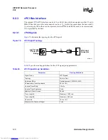
Page 116: ...ameters Figure 67 SPCI Address Data Signal Topology B3962 01 Ingress Intel 82559 NIC Egress Intel 82559 NIC SWF Connector Intel 21154 PCI to PCI Bridge A B Media Connector C D PMC Connector E F G H I Table 42 SPCI Address Data Group Guidelines Sheet 1 of 2 Parameter Routing Guidelines Signal Group SPCI Address Data Topology Daisy Chain Reference Plane Dual referenced PWR SIG GND Characteristic Tra...

Page 117: ...ils Maximum Via Count per Signal 10 vias Table 42 SPCI Address Data Group Guidelines Sheet 2 of 2 Parameter Routing Guidelines Figure 68 SPCI Clock Signals Topology B0518 01 B SPCI Device Connector A Intel 21154 PCI to PCI Bridge RS Table 43 SPCI Clock Signals Group Guidelines Parameter Routing Guidelines Signal Group SPCI Clk Topology Point to Point Reference Plane Dual referenced PWR SIG GND Cha...

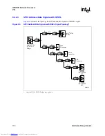
Page 118: ...Data Signals with IDSEL Figure 69 illustrates the topology for SPCI address data signals with IDSEL signal Figure 69 SPCI Address Data Signals with IDSEL Signal Topology1 1 Only the 211154 PCI PCI bridge case is shown Downloaded from Elcodis com electronic components distributor ...

Page 119: ...nal Trace Width 3 5 mils Nominal Trace Separation 9 mils Spacing to Other Groups 20 mils Trace Length A Maximum 2500 mils Trace Length B Maximum 1800 mils Trace Length C Maximum 200 mils Trace Length D Maximum 5200 mils Trace Length E Maximum 500 mils Trace Length F Maximum 7000 mils Trace Length G Maximum 200 mils Trace Length H Maximum 4500 mils Trace Length I Maximum 200 mils Trace Length J Max...

Page 120: ...PCI signal Table 45 provides routing guidelines for the cPCI signal group parameters Figure 70 cPCI Signal Topology B0520 01 Intel 21555 PCI to PCI Bridge CPCI Host Connector B A RS Table 45 cPCI Signal Group Guidelines Parameter Routing Guidelines Signal Group cPCI Signals Topology Point to Point Reference Plane Dual referenced PWR SIG GND Characteristic Trace Impedance 60 Ω 10 Nominal Trace Widt...

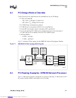
Page 121: ...uidelines 66 MHz four loads 33 MHz eight loads Figure 71 illustrates PCI bus topology for the IXDP2800 Advanced Development Platform 6 4 PCI Routing Examples IXP2800 Network Processor Figure 72 illustrates 64 bit PCI bus routing between processors and Figure 73 illustrates 64 bit PCI bus routing from the IXP28XX network processor to a bridge Figure 71 IXDP2800 PCI Bus Topology Block Diagram B3406 ...

Page 122: ...ardware Design Guide IXP28XX Network Processor PCI Figure 72 64 Bit PCI Bus Routing Between Processors 64 bit PCI bus routing between processors Downloaded from Elcodis com electronic components distributor ...
Page 123: ...tes 64 bit PCI bus routing from the IXP28XX network processor to the bridge Figure 73 64 bit PCI Bus Routing from IXP28XX Network Processor to Bridge 64 bit PCI bus routing from IXP28XX Network Processor to bridge Downloaded from Elcodis com electronic components distributor ...

Page 124: ...142 PCI_AD 0 6 118 0 241 PCI_AD 39 15 183 0 598 PCI_CBE_L 2 1 571 0 062 PCI_AD 1 7 934 0 312 PCI_AD 4 4 626 0 182 PCI_CBE_L 3 9 587 0 377 PCI_AD 10 11 996 0 472 PCI_AD 40 5 386 0 212 PCI_CBE_L 4 13 866 0 546 PCI_AD 11 16 187 0 637 PCI_AD 41 14 329 0 564 PCI_CBE_L 5 3 349 0 132 PCI_AD 12 2 379 0 094 PCI_AD 42 9 768 0 385 PCI_CBE_L 6 10 543 0 415 PCI_AD 13 10 843 0 427 PCI_AD 43 10 39 0 409 PCI_CBE_...

Page 125: ...PCI_AD 35 5 94 0 234 PCI_AD 8 10 682 0 421 SP_AD 0 15 47 0 609 PCI_AD 36 11 244 0 443 PCI_AD 9 12 02 0 473 SP_AD 1 9 926 0 391 PCI_AD 37 1 647 0 065 PCI_CBE_L 0 11 033 0 434 SP_AD 2 3 151 0 124 SP_AD 3 1 572 0 062 SP_AD 4 6 606 0 260 SP_AD 5 5 044 0 199 SP_AD 6 4 375 0 172 SP_AD 7 7 962 0 313 SP_ALE_L 3 457 0 136 SP_CLK 0 898 0 035 SP_CP 2 438 0 096 SP_CS_L 0 1 193 0 047 SP_CS_L 1 14 245 0 561 SP_...

Page 126: ...126 Hardware Design Guide IXP28XX Network Processor PCI Downloaded from Elcodis com electronic components distributor ...

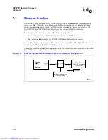
Page 127: ... Therefore an external set of buffers is needed to latch the address two chip selects are provided see Figure 74 note that the ACK signal is optional Note To meet interface timing requirements Intel suggests the external interface logic be implemented in a high speed CPLD Complex Programmable Logic Device as shown in Figure 77 Figure 74 Generic Slowport Connection A9318 02 SP_RD_L SP_CS_L 0 SP_CS_...

Page 128: ...t contains two types of interface and two ports Flash memory interface with a dedicated port used for the PROM device Microprocessor interface used for SONET SDH Framer Microprocessor access Access to each of these interfaces is differentiated by two chip selects SP_CS n External decode logic is required to latch the address and data Examples of the Slowport interface configuration on the IXP28XX ...

Page 129: ...ess IXP28XX Slowport Configuration Egress Intel IXP2800 Platform Figure 77 CPLD Implementation of a Flash EEPROM Interface B0183 01 Address Latches Address Latches Intel 8F128J3A 16 MByte 8 bit Flash SP_ALE A 9 2 A 17 10 A 24 18 D 7 0 CPLD A 1 0 SP_CLK SP_AD 7 0 NetROM Connector Address Latches Downloaded from Elcodis com electronic components distributor ...

Page 130: ...nal Name Description I O SP_AD 7 0 Address and Data multiplexed bidirectional tri state busses I O SP_OE_L Output enable for external buffer O SP_CP SP_A0 Latch enable for 16 or 32 bit data bus devices Address 0 for 8 bit devices O SP_DIR SP_A1 Data transaction direction Low for read High for write Address 1 for 8 bit devices O SP_ALE_L Address latch enable O SP_CS 1 0 Device Selects SP_CS 0 Lower...

Page 131: ...race Impedance 60 Ω 10 Nominal Trace Width 3 5 mils Nominal Trace Separation 9 mils Group spacing Isolation from other signal groups is 20 mils IXP28XX breakout guideline 4 mils with 4 mil space for a maximum of 300 mils Trace Length A Maximum 1500 mils Trace Length B Maximum 3500 mils Trace Length C Maximum 150 mils Trace Length D Maximum 100 mils Trace Length E Maximum 3000 mils Trace Length F M...

Page 132: ...deline Parameter Routing Guideline Signal Group Slowport Clock Topology Point to point Reference Plane Dual referenced PWR SIG GND Characteristic Trace Impedance 60 Ω 10 Nominal Trace Width 3 5 mils Nominal Trace Separation 9 mils Group spacing Isolation from other signal groups is 20 mils IXP28XX breakout guideline 4 mil with 4 mil space for a maximum of 300 mils Trace Length A Maximum 400 mils T...

Page 133: ...CS 1 Using these two signals the glue logic distinguishes between accesses to each interface Refer to the Intel IXP2800 Network Processor Hardware Reference Manual for additional details about the Slowport unit Figure 80 Slowport Address Data Topology Table 50 Slowport Address Data Routing Guidelines Parameter Routing Guideline Signal Group Address Data Topology Point to point Reference Plane Dual...

Page 134: ...t significant byte LSB of the address is delivered first and the most significant byte MSB is presented last Note Timing diagrams for all supported modes are provided in the Slowport unit section of the Intel IXP2800 Network Processor Hardware Reference Manual We recommend that you consult the HRM and review all of the timing diagrams in that section The Verilog code in Example 1 depicts an exampl...

Page 135: ...L A 24 2 Intel IXP2800 Network Processor SP_AD 7 0 SP_ALE_L SP_CLK SP_ACK_L CE CP D 7 0 A 24 18 A 17 10 A 9 2 Q 7 0 74f377 CE CP D 7 0 Q 7 0 74f377 OE_L Clock Driver CY2305 Figure 82 Mode 0 Single Write Transfer for a Fixed timed Device A9706 02 SP_CLK SP_ALE_L SP_CS_L 1 0 SP_WR_L D 7 0 A 1 0 17 10 24 18 9 2 17 10 24 18 9 2 SP_RD_L SP_A 1 0 SP_AD 7 0 2 0 4 6 8 10 12 14 16 18 20 Downloaded from Elc...

Page 136: ...ddress latch logic and data multiplexing and demultiplexing each section provides example implementations of the appropriate logic 7 1 2 2 1 Address Latch Logic The size of the address for the flash interface is fixed but is programmable in the microprocessor interface The Slowport address size data width control register SP_ADC configures the size of the address and data bus Since the address can...

Page 137: ...the data into the appropriate byte lane Another method would be to define the latched_add register to be 32 bits dropping any unused upper bits then ale_cnt would not be needed Example 3 shows a coded example of this logic Example 3 Microprocessor Address Latch Logic Without ale_cnt implementation of 32 bit address packing logic always posedge sp_clk begin if rst_l begin latched_add 32 h00000000 e...

Page 138: ...s and control which device drives the bus during read and write transactions Note The actual protocol of these control signals varies depending on the interface configuration mode 1 2 3 or 4 The remainder of this section concentrates on the Mode 3 protocol the mode that would be used to interface to the Intel IXF1010 10 port 100 1000Mbps Ethernet MAC Figure 84 shows an example of discrete componen...

Page 139: ...R 9 0 DATA 15 0 Intel IXP2800 Network Processor Intel or AMCC SONET SDH SP_ALE_L SP_CLK SP_CP SP_OE_L SP_DIR ALE CE CP D 7 0 ADDR 10 8 ADDR 7 1 DATA 7 0 DATA 15 8 VCC Q 7 0 74F377 D 7 0 CPAB 74F646 DIR OE CPBA SAB O 7 0 SBA D 7 0 CPAB 74F646 DIR OE CPBA SAB O 7 0 SBA VCC Other names and brands may be claimed as property of others MCUTYPE VCC Clock Driver CY2305 Downloaded from Elcodis com electron...

Page 140: ...he data is shifted into a register implemented in the glue logic device from least significant byte LSB through most significant byte MSB Note The IXP28XX CSR Transmit Enable Register SP_TXE can be used to delay the data and relevant Slowport signals in relation to the SP_CLK For programming information refer to the Intel IXP2800 Network Processor Hardware Reference Manual Figure 85 Mode 3 32 Bit ...

Page 141: ...l begin data 31 0 uP_rd_data end end else if sp_oe_l sp_rd_l end always posedge spa 0 In the Example 4 code the 32 bit register used for latching the write data is also used for latching the read data decreasing the number of gates needed for implementing the glue logic If desired separate registers for latching the write and read data can be used in this case the rising edge of the SP_RD_L signal...

Page 142: ...ta coming from the downstream device on the rising edge of the read signal or as specified by the device Figure 87 shows the timing of the Slowport interface signals presented to the glue logic during a read transaction Note The IXP28XX CSR Receive Enable Register SP_RXE can be used to advance the data sampled internally before the rising edge of the SP_CLK For programming SP_RXE refer to the Inte...

Page 143: ... signal is asserted PACK_CNT is cleared if SHIFT_EN is de asserted This procedure ensures that PACK_CNT will be zero at the beginning of each read cycle As the count increments the appropriate byte is driven onto the SP_RD_OUT bus as SP_CP is pulsed to complete the 32 bit transfer The SHIFT_EN control signal detects if the SP_OE_L signal is asserted the SP_RD_L signal is de asserted and the SP_DIR...

Page 144: ...de depicts an example implementation of the data unpacking logic implementation of pack_cnt control logic the count is incremented on each rising edge of sp_a 0 if shift_en is active always posedge sp_a 0 begin if rst_l begin pack_cnt 2 b00 end else begin if shift_en begin pack_cnt pack_cnt 1 end else if shift_en begin pack_cnt 2 b00 end end else if rst_l end always posedge sp_clk Implementation o...

Page 145: ... is a complete implementation and can be easily modified to support the other three values The data packing unpacking logic examples were chosen to provide an interface to an Intel AMCC device While the other modes have subtle protocol and interface signal differences the logic used for address latching and data packing unpacking should be essentially the same Again the example uses the 32 bit cas...

Page 146: ...146 Hardware Design Guide IXP28XX Network Processor Slowport Downloaded from Elcodis com electronic components distributor ...

Page 147: ... 650 MHz RPIXP2800BA B1 Q808 MM 861093 1 0 GHz RPIXP2800BB B1 Q809 MM 861099 1 4 GHz RPIXP2800BC B1 NA1 MM 862907 650 MHz RPIXP2800BA B1 NA1 MM 862117 1 0 GHz RPIXP2800BB B1 NA1 MM 855650 1 4 GHz RPIXP2850BA B0 Q670 MM 858140 1 0 GHz RPIXP2850BB B0 Q671 MM 858141 1 4 GHz RPIXP2850BC B1 Q854 MM 862908 650 MHz RPIXP2850BA B1 Q810 MM 861102 1 0 GHz RPIXP2850BB B1 Q811 MM 861132 1 4 GHz RPIXP2850BC B1...

Page 148: ...ntry of Origin 2D Matrix RPIXP2800xx FPO INTEL XXXX PHILIPPINES M C encoded assembly lot traceability mark Figure 90 Intel IXP2850 Network Processor Package Marking B0565 01 Level 1 Name Intel Legal Country of Origin 2D Matrix RPIXP2850xx FPO INTEL XXXX PHILIPPINES M C encoded assembly lot traceability mark Downloaded from Elcodis com electronic components distributor ...

Page 149: ...cessor Package Ball Grid Array A9208 03 S1 Pin 1 corner øb S2 e e AU AT AR AP AN AM AL AK AJ AH AG AF AE AD AC AB AA Y W V U T R P N M L K J H G F E D C B A 1 2 3 4 5 6 7 8 9 10 11 12 13 14 15 16 17 18 19 20 21 22 23 24 25 26 27 28 29 30 31 32 33 34 35 36 37 Bottom Pin side View Figure 92 Intel IXP2800 or Intel IXP2850 Network Processor Package Side View A9209 02 Side View A3 Seating Plane A A1 C ...

Page 150: ... Intel IXP2800 or IXP2850 Network Processor Package Dimensions Symbol Minimum Maximum A 3 891 4 565 A1 0 40 0 60 A3 2 266 2 49 b 0 61 C 1 225 1 475 D 37 45 37 55 E 37 45 37 55 F1 33 4 33 6 F2 33 4 33 6 e 1 00 S1 0 750 S2 0 750 Note All dimensions are in millimeters mm A9207 02 Top View E F1 D F2 Downloaded from Elcodis com electronic components distributor ...

Page 151: ...les processor power on 30 Droop analysis di dt 31 F Flash memory Slowport 133 PROM Slowport 134 address latch 134 Flow Control Bus MSF 103 I Input timing processor 64 Interface topologies 81 L LC filter network 26 Loopback length QDRII SRAM 85 LVDS interface design review checklist 104 routing example 105 signals routing 104 simulation results 106 trace characteristics for IXDP2800 platform 104 re...

Page 152: ...control topologies RPE WPE BWE 76 DataIn topology 70 DataOut topology 68 design review checklist 94 interface 57 output timing specifications 64 placement with TCAM 90 routing 84 alternating layers 89 recommendations 84 rules 65 with TCAM 93 recommendations 92 using x9 versus x18 parts 58 VREF generation 79 trace requirements 65 QDRII SRAM Loopclock length 85 R Rambus channel design 35 controller ...

Page 153: ...ogy 70 DataOut topology 68 design review checklist 94 interface 57 output timing specifications 64 placement with TCAM 90 routing 84 alternating layers 89 rules 65 with TCAM 93 recommendations 92 using x9 versus x18 parts 58 VREF generation 79 QDRII Loopback length 85 Supply voltage power up sequence 24 System overview 11 T TCAM interface 81 base card side 81 placement with QDR SRAM 90 routing wit...

Page 154: ...Index 154 Downloaded from Elcodis com electronic components distributor ...

Reviews: