136
Hardware Design Guide
IXP28XX Network Processor
Slowport
7.1.2.2
Microprocessor Interface Logic
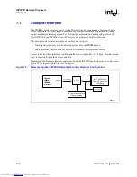
The Slowport microprocessor interface can be configured to support 8-, 16-, and 32-bit devices.
Refer to the
Intel® IXP2400 and IXP2800 Network Processor Programmer’s Reference Manual
for detailed information about each mode.
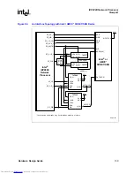
As with the flash interface, external logic must be implemented to latch the address. Since this
interface can also support 8-, 16-, and 32-bit devices, external logic must also be implemented to
perform the packing and unpacking of the read and write data when configured for 16- and 32-bit
mode. To control the packing and unpacking of data and steer the direction of the bus, the
microprocessor interface provides three additional signals: SP_CP, SP_OE_L, and SP_DIR.
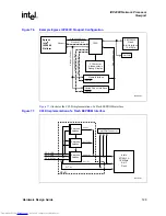
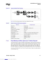
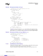
The logic required to latch the address is the same as the logic described in
Figure 81
for the flash
interface. The following sections describe the differences from the flash interface as they pertain to
the address latch logic and data multiplexing and demultiplexing; each section provides example
implementations of the appropriate logic.
7.1.2.2.1
Address Latch Logic
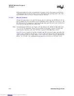
The size of the address for the flash interface is fixed, but is programmable in the microprocessor
interface. The Slowport address size/data width control register, SP_ADC, configures the size of
the address and data bus. Since the address can be 8-, 16-, 24-, or 25-bits wide, the number of clock
cycles required to latch the address could be as many as four for the 25-bit case, and as few as one
for the 8-bit case. The mechanism for latching the address is the same: on the rising edge of
SP_CLK if SP_ALE_L is asserted. The number of clock cycles in which SP_ALE_L is asserted
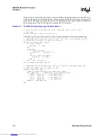
varies and depends on the programmed address size. The address logic implemented for the flash
interface could be modified for the microprocessor interface as depicted in
Example 2
.
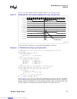
Figure 83.
Mode 0 Single Write Transfer for a Self-timing Device
A9707-02
SP_CLK
SP_ALE_L
SP_CS_L
[1:0]
SP_WR_L
D[7:0]
A[1:0]
24:18
17:10
9:2
24:18
17:10
9:2
SP_RD_L
SP_A[1:0]
SP_AD[7:0]
SP_ACK_L
2
0
4
6
8
10
12
14
16
18
20
Downloaded from
Elcodis.com
electronic components distributor

