Hardware Design Guide
79
IXP28XX Network Processor
QDR SRAM
Table 32
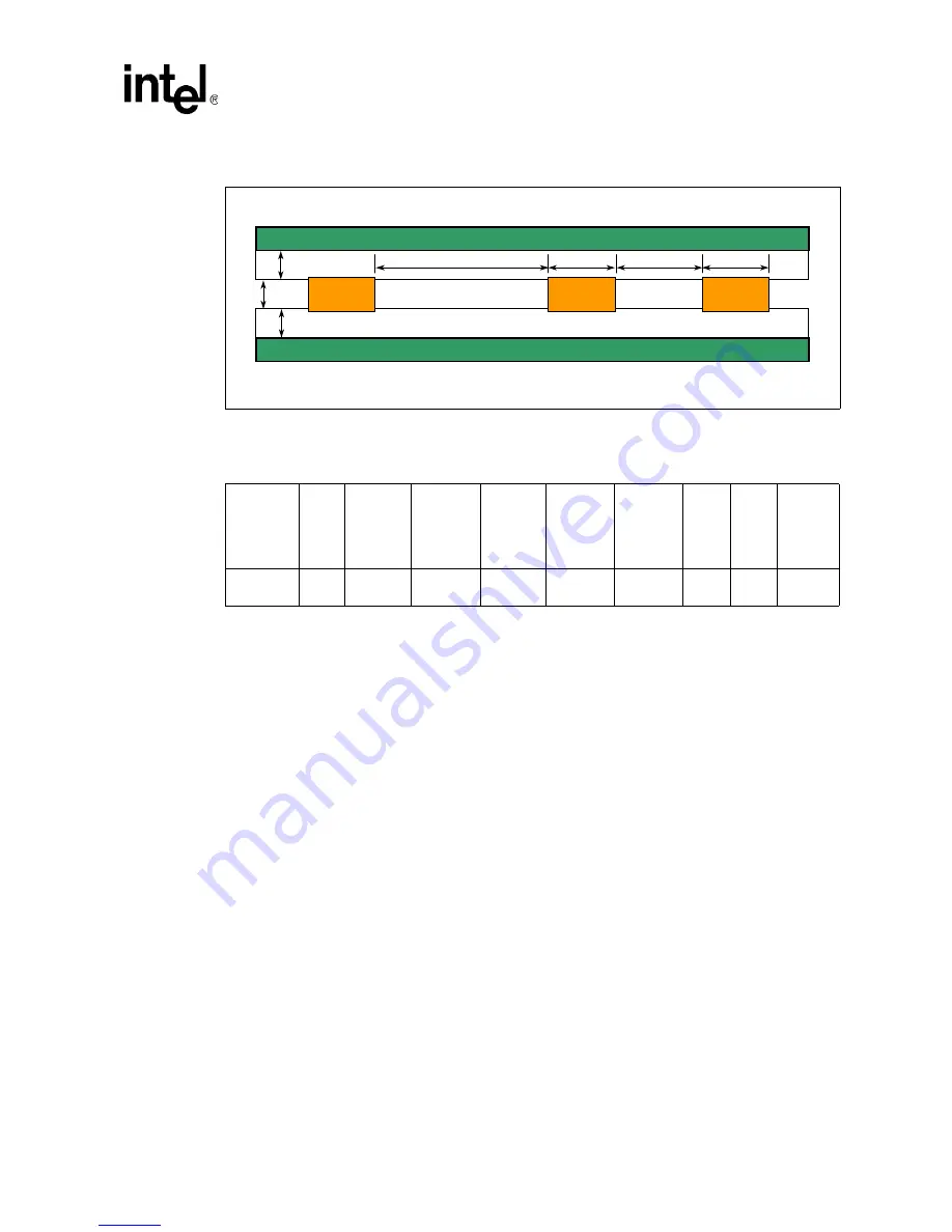
lists the QDR CONTROL stack-up signal cross-section details.
4.6
QDR SRAM V
REF
Generation
The best known method for V
REF
generation is to derive the 0.75-V reference through a resistive
divider from the 1.5-V QDR supply. The following solutions can be used to generate the V
REF
supply:
•
Figure 42
depicts a circuit that creates V
REF
through a resistive divider which is then fed
through an optical amplifier to create a noise-sensitive voltage reference.
•
Figure 43
and
Figure 44
show a resistor divider circuit to generate the V
REF
supply.
Figure 41.
Control BWE# Signal Trace Width/Spacing Routing
!
!
POWER or GND Plane
POWER or GND Plane
Table 32.
QDR CONTROL Stack-up Signal Cross-section Details
Parameter
QDR
Signal
Trace
Width (W)
[mils]
Trace
Thickness
(Tsignal)
[mils]
Trace
Spacing
(S) [mils]
D1
Thickness
(TD1)
[mils]
D2
Thickness
(Td2)
[mils]
Er(D1) Er(D2)
Spacing
between
signal
groups
[mils]
Value
CONT
ROL
5
0.5
8 - 15
5.0
5.7
3.5
3.8
20 - 25
Downloaded from
Elcodis.com
electronic components distributor


