6-3
RANGE REGISTERS
6.3.
MEMORY TYPE DESCRIPTIONS
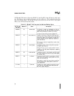
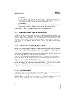
This section provides detailed descriptions of the Pentium Pro processor’s memory types: UC,
WC, WT, WP, and WB.
6.3.1.
UC Memory Type
The UC (uncacheable) memory type provides an uncacheable memory space. The processor’s
accesses to UC memory are executed in program order, without reordering. Accesses to other
memory types can pass accesses to UC memory.
6.3.2.
WC Memory Type
The WC (write-combining) memory type provides a write-combining buffering strategy for
write operations, useful for frame buffers.
Writes to WC memory can be buffered and combined in the processor’s write-combining buffers
(WCB). The WCBs are viewed as a special-purpose outgoing write buffers, rather than a cache.
The WCBs are written to memory to allocate a different address, or they are written to memory
after leaving an interrupt, or executing a serializing, locked, or I/O instruction. There are no or-
dering constraints on the writing of WCBs to memory.
The Pentium Pro processor uses line size WCBs. WCB to memory writes use a single Memory
Write Transaction (W/WB# = 1) of 32 bytes if all WCB bytes are valid. If all WCB bytes are not
valid, the valid bytes are written to memory using a series of <= 8 byte Memory Write Transac-
tions. Such a series of transactions can be issued in any order regardless of the program order in
which the write data was generated. Therefore, WC memory is a weakly ordered memory type.
A particular Memory Write Transaction can write discontiguous bytes within an 8-byte span.
External hardware that supports the WC memory type must support such writes.
6.3.3.
WT Memory Type
The WT (write-through) memory type reads data in lines and caches read data, but maps all
writes to the bus, while updating the cache to maintain cache coherency.
Writes directed at WT memory can be split across 32-byte and 8-byte boundaries, but are never
combined.
The Pentium Pro processor implementation of writes to WT memory updates valid lines in the
L1 data cache and invalidates valid lines in the L2 cache and in the L1 code cache.
Summary of Contents for Pentium Pro Family
Page 17: ...1 Component Introduction ...
Page 26: ...2 Pentium Pro Processor Architecture Overview ...
Page 27: ......
Page 36: ...3 Bus Overview ...
Page 62: ...4 Bus Protocol ...
Page 105: ...5 Bus Transactions and Operations ...
Page 126: ...6 Range Registers ...
Page 131: ...7 Cache Protocol ...
Page 135: ...8 Data Integrity ...
Page 148: ...9 Configuration ...
Page 161: ...10 Pentium Pro Processor Test Access Port TAP ...
Page 172: ...11 Electrical Specifications ...
Page 201: ...12 GTL Interface Specification ...
Page 229: ...13 3 3V Tolerant Signal Quality Specifications ...
Page 233: ...14 Thermal Specifications ...
Page 239: ...15 Mechanical Specifications ...
Page 241: ...15 2 MECHANICAL SPECIFICATIONS s Figure 15 1 Package Dimensions Bottom View ...
Page 252: ...16 Tools ...
Page 260: ...16 8 TOOLS Figure 16 4 Generic MP System Layout for Debug Port Connection ...
Page 264: ...17 OverDrive Processor Socket Specification ...
Page 290: ...A Signals Reference ...
Page 320: ...Index ...
Page 328: ......

