11-1
CHAPTER 11
ELECTRICAL SPECIFICATIONS
11.1.
THE PENTIUM
®
PRO PROCESSOR BUS AND VREF
Most of the Pentium Pro processor signals use a variation of the low voltage GTL signaling
technology (Gunning Transceiver Logic).
The Pentium Pro processor bus specification is similar to the GTL specification but has been
enhanced to provide larger noise margins and reduced ringing. This is accomplished by increas-
ing the termination voltage level and controlling the edge rates. Because this specification is dif-
ferent from the standard GTL specification, we will refer to the new specification as GTL+ in
this document.
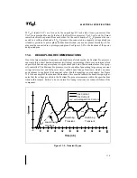
The GTL+ signals are open-drain and require external termination to a supply that provides the
high signal level. The GTL+ inputs use differential receivers which require a reference signal
(VREF). Termination (Usually a resistor on each end of the signal trace) is used to pull the bus
up to the high voltage level and to control reflections on the stub-free transmission line. VREF
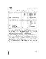
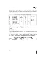
is used by the receivers to determine if a signal is a logical 0 or a logical 1. See Table 11-8
for the bus termination specifications for GTL+, and Chapter 12, GTL+ Interface Specifi-
cation for the GTL+ Interface Specification.
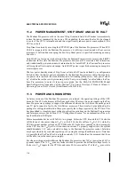
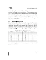
There are 8 VREF pins on the Pentium Pro processor to ensure that internal noise will not affect
the performance of the I/O buffers. Pins A1, C7, S7 and Y7 (VREF[3:0]) must be tied together
and pins A47, U41, AE47 and AG45 (VREF[7:4]) must be tied together. The two groups may
also be tied to each other if desired.
The GTL+ bus depends on incident wave switching. Therefore timing calculations for GTL+
signals are based on flight time as opposed to capacitive deratings. Analog signal simulation of
the Pentium Pro processor bus including trace lengths is highly recommended when designing
a system with a heavily loaded GTL+ bus. See Intel’s technical documents on the world wide
web page (http:\\www.intel.com) to down-load the buffer models for the Pentium Pro processor
in IBIS format.
Figure 11-1. GTL+ Bus Topology
CPU
CPU
ASIC
ASIC
CPU
CPU
1.5V
1.5V
No stubs
Summary of Contents for Pentium Pro Family
Page 17: ...1 Component Introduction ...
Page 26: ...2 Pentium Pro Processor Architecture Overview ...
Page 27: ......
Page 36: ...3 Bus Overview ...
Page 62: ...4 Bus Protocol ...
Page 105: ...5 Bus Transactions and Operations ...
Page 126: ...6 Range Registers ...
Page 131: ...7 Cache Protocol ...
Page 135: ...8 Data Integrity ...
Page 148: ...9 Configuration ...
Page 161: ...10 Pentium Pro Processor Test Access Port TAP ...
Page 172: ...11 Electrical Specifications ...
Page 201: ...12 GTL Interface Specification ...
Page 229: ...13 3 3V Tolerant Signal Quality Specifications ...
Page 233: ...14 Thermal Specifications ...
Page 239: ...15 Mechanical Specifications ...
Page 241: ...15 2 MECHANICAL SPECIFICATIONS s Figure 15 1 Package Dimensions Bottom View ...
Page 252: ...16 Tools ...
Page 260: ...16 8 TOOLS Figure 16 4 Generic MP System Layout for Debug Port Connection ...
Page 264: ...17 OverDrive Processor Socket Specification ...
Page 290: ...A Signals Reference ...
Page 320: ...Index ...
Page 328: ......

