11-8
ELECTRICAL SPECIFICATIONS
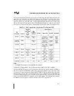
Support for a wider range of VID settings will benefit the system in meeting the power require-
ments of future Pentium Pro processors. Note that the ‘1111’ (or all opens) ID can be used to
detect the absence of a processor in a given socket as long as the power supply used does not
affect these lines.
To use these pins, they may need to be pulled up by an external resistor to another power source.
The power source chosen should be one that is guaranteed to be stable whenever the supply to
the voltage regulator is stable. This will prevent the possibility of the Pentium Pro processor sup-
ply running up to 3.5V in the event of a failure in the supply for the VID lines. Note that the
specification for the standard Pentium Pro processor Voltage Regulator Modules allows the use
of these signals either as TTL compatible levels or as opens and shorts. Using them as TTL com-
patible levels will require the use of pull-up resistors to 5V if the input voltage to the regulator
is 5V and the use of a voltage divider if the input voltage to the regulator is 12V. The resistors
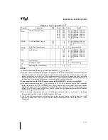
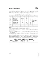
chosen should not cause the current through a VID pin to exceed its specification in Table 11-3.
There must not be any other components on these signals if the VRM uses them as opens and
shorts.
11.7.
JTAG CONNECTION
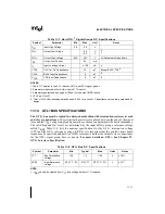
The Debug Port described in Section 16.2., “In-Target Probe for the Pentium® Pro Processor
(ITP)” should be at the start and end of the JTAG chain with TDI to the first component coming
from the Debug Port and TDO from the last component going to the Debug Port. The recom-
mended pull-up value for Pentium Pro processor TDO pins is 240
Ω
.
Due to the voltage levels supported by the Pentium Pro processor JTAG logic, it is recommend-
ed that the Pentium Pro processors and any other 3.3V components be first in the JTAG chain.
A translation buffer should be used to connect to the rest of the chain unless a 5V component
can be used next that is capable of accepting a 3.3V input. Similar considerations must be made
for TCK, TMS and TRST#. Components may need these signals buffered to match required log-
ic levels.
In a multi-processor system, be cautious when including empty Pentium Pro processor sockets
in the scan chain. All sockets in the scan chain must have a processor installed to complete the
chain or the system must support a method to bypass the empty sockets.
See Section 16.2., “In-Target Probe for the Pentium® Pro Processor (ITP)” for full information
on placing a Debug Port in the JTAG chain.
Summary of Contents for Pentium Pro Family
Page 17: ...1 Component Introduction ...
Page 26: ...2 Pentium Pro Processor Architecture Overview ...
Page 27: ......
Page 36: ...3 Bus Overview ...
Page 62: ...4 Bus Protocol ...
Page 105: ...5 Bus Transactions and Operations ...
Page 126: ...6 Range Registers ...
Page 131: ...7 Cache Protocol ...
Page 135: ...8 Data Integrity ...
Page 148: ...9 Configuration ...
Page 161: ...10 Pentium Pro Processor Test Access Port TAP ...
Page 172: ...11 Electrical Specifications ...
Page 201: ...12 GTL Interface Specification ...
Page 229: ...13 3 3V Tolerant Signal Quality Specifications ...
Page 233: ...14 Thermal Specifications ...
Page 239: ...15 Mechanical Specifications ...
Page 241: ...15 2 MECHANICAL SPECIFICATIONS s Figure 15 1 Package Dimensions Bottom View ...
Page 252: ...16 Tools ...
Page 260: ...16 8 TOOLS Figure 16 4 Generic MP System Layout for Debug Port Connection ...
Page 264: ...17 OverDrive Processor Socket Specification ...
Page 290: ...A Signals Reference ...
Page 320: ...Index ...
Page 328: ......


