background image

4-23

BUS PROTOCOL

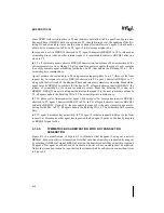
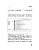
In T1, there are no transactions outstanding on the bus and {scnt} is 0. In T2, transaction 1 is
issued. In T4, as a result of the transaction driven in T2, {scnt} is incremented.

In T5, transaction 2 is issued. In T6, which is four clocks after the corresponding ADS# in T2,
the snoop results for transaction 1 are driven. In T7, {scnt} is incremented indicating that there
are two transactions on the bus that have not completed the Snoop Phase. Also in T7, the snoop
results for transaction 1 are observed. As a result, in T8, {scnt} is decremented.

In T8, the third transaction is issued. Two clocks later in T10, {scnt} is incremented. In T11,
{scnt} is decremented because the snoop results from transaction 2 are observed in T10.

In T13, the snoop results for transaction 3 are observed and in T14 {scnt} is again decremented.

4.4.2.2.

STALLED SNOOP PHASE

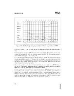
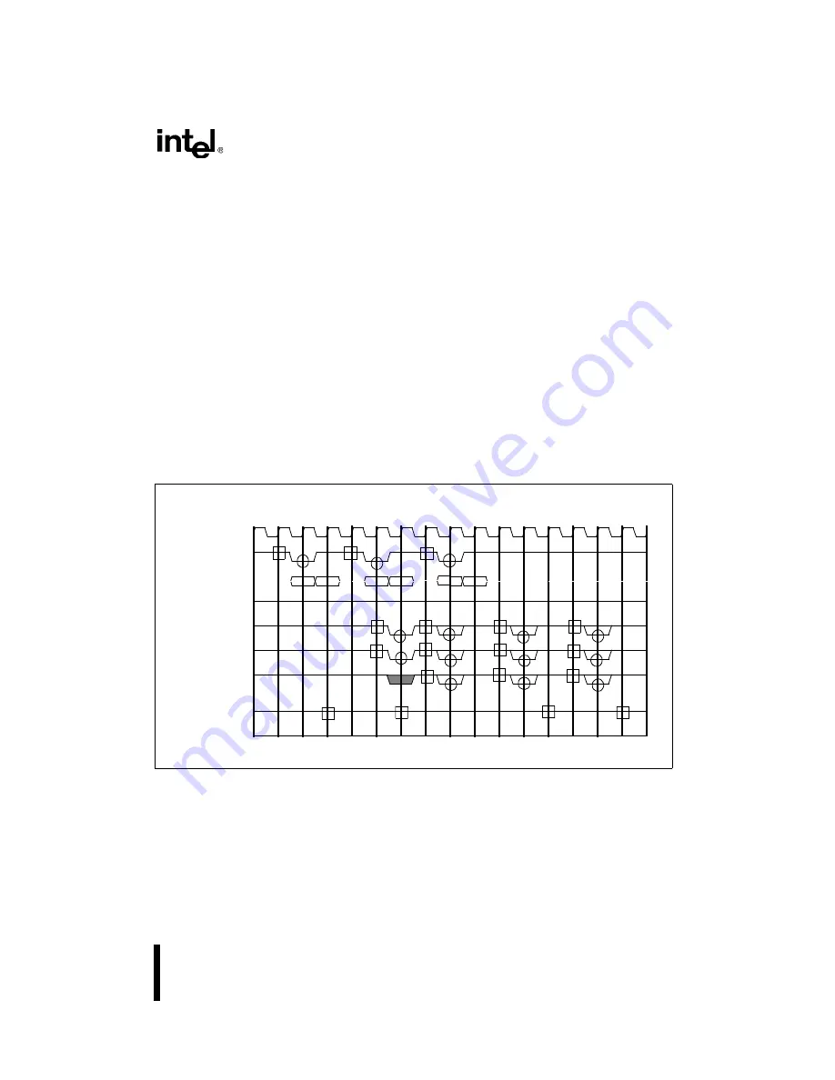
Figure 4-13 illustrates how a slower snooping agent can delay the Snoop Phase if it is unable to
deliver valid snoop results within four clocks after ADS# is asserted. The figure also illustrates
that the snoop phase of subsequent trasactions are also stalled and occur two clocks late due to
the stall of transaction one’s snoop phase.

Transactions 1, 2 and 3 are initiated with ADS# activation in T2, T5, and T8.

The Snoop Phase for transaction 1 begins in T6 four clocks from ADS#. All agents capable of
driving valid snoop response in four clocks drive appropriate levels on the snoop signals HIT#,
HITM#, and DEFER#. A slower agent that is unable to generate a snoop response in four clocks
asserts both HIT# and HITM# together in T6 to extend the Snoop Phase. Note that if the Snoop

Figure 4-13.  Snoop Phase Stall Due to a Slower Agent

CLK

ADS#

{REQUEST}

HITM#

AERR#

HIT#

A

AA

AAAAAA

AA

A

AAAAAA

A

A

AAA

AA

A

AAAA

A

A

AAA

A

A

AAAAAA

 1

2

3

4

5

6

7

8

9  

10

11

12

13

14

15

16

AA

AA

AAAAAA

A

A

AAAAAA

A

A

AAAAAA

AA

AA

AAAAAA

 2

 3

AA

A

AAAA


 2

 2

3

AA

A

AAAA

A

A

AAA

DEFER#


3

2

2

3

3

0

0

0

1

1

1

2

2

2

2

2

2

1

1

1

0

{scnt}

Summary of Contents for Pentium Pro Family

Page 1: ...tium Pro Family Developer s Manual consists of three books Specifications Order Number 242690 Programmer s Reference Manual Order Number 242691 and the Operating System Writer s Guide Order Number 242692 Please refer to all three volumes when evaluating your design needs 1996 ...

Page 2: ...cept as provided in Intel s Terms and Conditions of Sale for such products No license express or implied by estoppel or otherwise to any intellectual property rights is granted herein Intel retains the right to make changes to these specifications at any time without notice Microcomputer Products may have minor variations to this specification known as errata Other brands and names are the propert...

Page 3: ... 2 8 CHAPTER 3 BUS OVERVIEW 3 1 SIGNAL AND DIAGRAM CONVENTIONS 3 1 3 2 SIGNALING ON THE PENTIUM PRO PROCESSOR BUS 3 2 3 3 PENTIUM PRO PROCESSOR BUS PROTOCOL OVERVIEW 3 4 3 3 1 Transaction Phase Description 3 4 3 3 2 Bus Transaction Pipelining and Transaction Tracking 3 6 3 3 3 Bus Transactions 3 7 3 3 4 Data Transfers 3 8 3 3 4 1 Line Transfers 3 9 3 3 4 2 Part Line Aligned Transfers 3 9 3 3 4 3 P...

Page 4: ...1 5 Symmetric Agent Arbitration Protocol Rules 4 16 4 1 5 1 Reset Conditions 4 16 4 1 5 2 Bus Request Assertion 4 16 4 1 5 3 Ownership from Idle State 4 16 4 1 5 4 Ownership from Busy State 4 17 4 1 5 4 1 Bus Parking and Release with a Single Bus Request 4 17 4 1 5 4 2 Bus Exchange with Multiple Bus Requests 4 17 4 1 6 Priority Agent Arbitration Protocol Rules 4 17 4 1 6 1 Reset Conditions 4 17 4 ...

Page 5: ...Transaction 4 34 4 6 2 3 Implicit Writeback 4 35 4 6 2 4 Full Speed Read Partial Transactions 4 36 4 6 2 5 Relaxed DBSY Deassertion 4 37 4 6 2 6 Full Speed Read Line Transfers Same Agent 4 38 4 6 2 7 Full Speed Write Partial Transactions 4 39 4 6 2 8 Full Speed Write Line Transactions Same Agents 4 40 4 6 3 Data Phase Protocol Rules 4 42 4 6 3 1 Valid Data Transfer 4 42 4 6 3 2 Request Initiated D...

Page 6: ... 3 3 Deferred Operations 5 16 5 3 3 1 Response Agent Responsibilities 5 17 5 3 3 2 Requesting Agent Responsibilities 5 18 5 3 4 Locked Operations 5 19 5 3 4 1 Split Bus Lock 5 20 CHAPTER 6 RANGE REGISTERS 6 1 INTRODUCTION 6 1 6 2 RANGE REGISTERS AND PENTIUM PRO PROCESSOR INSTRUCTION EXECUTION 6 1 6 3 MEMORY TYPE DESCRIPTIONS 6 3 6 3 1 UC Memory Type 6 3 6 3 2 WC Memory Type 6 3 6 3 3 WT Memory Typ...

Page 7: ...ion Policy 9 3 9 1 7 BERR Driving Policy for Initiator Bus Errors 9 3 9 1 8 BERR Driving Policy for Target Bus Errors 9 4 9 1 9 Bus Error Driving Policy for Initiator Internal Errors 9 4 9 1 10 BERR Observation Policy 9 4 9 1 11 BINIT Driving Policy 9 4 9 1 12 BINIT Observation Policy 9 4 9 1 13 In order Queue Pipelining 9 4 9 1 14 Power on Reset Vector 9 5 9 1 15 FRC Mode Enable 9 5 9 1 16 APIC M...

Page 8: ...SPECIFICATIONS 11 17 11 15 A C SPECIFICATIONS 11 18 11 16 FLEXIBLE MOTHERBOARD RECOMMENDATIONS 11 28 CHAPTER 12 GTL INTERFACE SPECIFICATION 12 1 SYSTEM SPECIFICATION 12 1 12 1 1 System DC Parameters 12 2 12 1 2 Topological Guidelines 12 4 12 1 3 System AC Parameters Signal Quality 12 4 12 1 3 1 Ringback Tolerance 12 6 12 1 4 AC Parameters Flight Time 12 8 12 2 GENERAL GTL I O BUFFER SPECIFICATION ...

Page 9: ...s 16 2 16 2 4 Signal Notes 16 3 16 2 4 1 Signal Note 1 RESET PRDYx 16 4 16 2 4 2 Signal Note 2 DBRESET 16 4 16 2 4 3 Signal Note 3 POWERON 16 4 16 2 4 4 Signal Note 4 DBINST 16 4 16 2 4 5 Signal Note 5 TDO and TDI 16 4 16 2 4 6 Signal Note 6 PREQ 16 4 16 2 4 7 Signal Note 7 TRST 16 5 16 2 4 8 Signal Note 8 TCK 16 5 16 2 4 9 Signal Note 9 TMS 16 6 16 2 5 Debug Port Layout 16 7 16 2 5 1 Signal Quali...

Page 10: ...ng Requirements 17 18 17 5 4 Thermal Equations and Data 17 18 17 6 CRITERIA FOR OVERDRIVE PROCESSOR 17 19 17 6 1 Related Documents 17 20 17 6 2 Electrical Criteria 17 20 17 6 2 1 OverDrive Processor Electrical Criteria 17 20 17 6 2 2 Pentium Pro Processor Electrical Criteria 17 22 17 6 3 Thermal Criteria 17 22 17 6 3 1 OverDrive Processor Cooling Requirements Systems Testing Only 17 22 17 6 3 2 Pe...

Page 11: ... I O A 12 A 1 26 EXF 4 0 I O A 13 A 1 27 FERR O A 13 A 1 28 FLUSH I A 13 A 1 29 FRCERR I O A 14 A 1 30 HIT I O HITM I O A 14 A 1 31 IERR O A 15 A 1 32 IGNNE I A 15 A 1 33 INIT I A 15 A 1 34 INTR I A 16 A 1 35 LEN 1 0 I O A 16 A 1 36 LINT 1 0 I A 16 A 1 37 LOCK I O A 17 A 1 38 NMI I A 17 A 1 39 PICCLK I A 17 A 1 40 PICD 1 0 I O A 17 A 1 41 PWR_GD I A 18 A 1 42 REQ 4 0 I O A 18 A 1 43 RESET I A 19 A...

Page 12: ... 4 15 Figure 4 11 Request Generation Phase 4 19 Figure 4 12 Four Clock Snoop Phase 4 22 Figure 4 13 Snoop Phase Stall Due to a Slower Agent 4 23 Figure 4 14 RS 2 0 Activation with no TRDY 4 27 Figure 4 15 RS 2 0 Activation with Request Initiated TRDY 4 28 Figure 4 16 RS 2 0 Activation with Snoop Initiated TRDY 4 29 Figure 4 17 RS 2 0 Activation After Two TRDY Assertions 4 30 Figure 4 18 Request In...

Page 13: ...Rising Edge Slower Than 0 3V ns 12 10 Figure 12 7 Extrapolated Flight Time of a Non Monotonic Rising Edge 12 11 Figure 12 8 Extrapolated Flight Time of a Non Monotonic Falling Edge 12 11 Figure 12 9 Acceptable Driver Signal Quality 12 16 Figure 12 10 Unacceptable Signal Due to Excessively Slow Edge After Crossing VREF 12 16 Figure 12 11 Test Load for Measuring Output AC Timings 12 18 Figure 12 12 ...

Page 14: ...es and Adjacent Voltage Regulator Module 17 2 Figure 17 2 OverDrive Processor Pinout 17 3 Figure 17 3 OverDrive Processor Envelope Dimensions 17 5 Figure 17 4 Space Requirements for the OverDrive Processor 17 7 Figure 17 5 Header 8 Pinout 17 9 Figure 17 6 OverDrive Voltage Regulator Module Envelope 17 11 Figure 17 7 Upgrade Presence Detect Schematic Case 1 17 12 Figure 17 8 Upgrade Presence Detect...

Page 15: ...Configuration for the Pentium Pro Processor 9 5 Table 9 2 BREQ 3 0 Interconnect 9 6 Table 9 3 Arbitration ID Configuration 9 8 Table 9 4 Bus Frequency to Core Frequency Ratio Configuration1 9 9 Table 9 5 Pentium Pro Processor Power on Configuration Register 9 10 Table 9 6 Pentium Pro Processor Power on Configuration Register APIC Cluster ID bit Field 9 11 Table 9 7 Pentium Pro Processor Power on C...

Page 16: ... Header 8 Pin Reference 17 10 Table 17 3 OverDrive Processor CPUID 17 14 Table 17 4 OverDrive Processor D C Specifications 17 15 Table 17 5 OverDrive VRM Specifications 17 16 Table 17 6 OverDrive VRM Power Dissipation for Thermal Design 17 18 Table 17 7 OverDrive Processor Thermal Resistance and Maximum Ambient Temperature 17 19 Table 17 8 Electrical Test Criteria for Systems Employing Header 8 17...

Page 17: ...1 Component Introduction ...

Page 18: ...h speed bus The Pentium Pro processor may be upgraded by a future OverDrive processor and matching voltage regulator module described in Chapter 17 OverDrive Processor Socket Specification Since increasing clock frequencies and silicon density can complicate system designs the Pen tium Pro processor integrates several system components which alleviate some of the previous system requirements The s...

Page 19: ...Pentium Pro processor cache protocol complexity is handled by the processor A non caching I O bridge on the Pentium Pro processor bus does not need to recognize the cache protocol and does not need snoop logic The I O bridge can issue standard memory accesses on the Pentium Pro processor bus which are transparently snooped by all Pentium Pro processor bus agents If data is modified in a Pentium Pr...

Page 20: ...and a combination of four other loads consisting primarily of bus clusters memory controllers I O bridges and custom attachments In a four processor system the data bus is the most critical resource To account for this situa tion the Pentium Pro processor bus implements several features to maximize available bus bandwidth including pipelined transactions in which bus transactions in different phas...

Page 21: ... the smallest depth supported by any agent processors memory or I O The Pentium Pro processor bus can be configured at power on to support a maximum of eight outstanding bus transactions depending on the amount of buffering available in the system Each Pentium Pro processor is capable of issuing up to four outstanding transactions The Pentium Pro processor bus enables transactions with long latenc...

Page 22: ...Pro processor to be used in high data integrity fault tolerant applications In addition two Pentium Pro processors can be configured at power on as an FRC pair or a multiprocessor ready pair 1 3 SYSTEM OVERVIEW Figure 1 2 illustrates the Pentium Pro processor system environment containing multiple pro cessors MP memory and I O This particular architectural view is not intended to imply any impleme...

Page 23: ...e of the signal when driven low For example when FLUSH is low a flush has been requested When NMI is high a Non maskable interrupt has occurred In the case of lines where the name does not imply an active state but describes part of a binary sequence such as address or data the symbol implies that the signal is inverted For example D 3 0 HLHL refers to a hex A and D 3 0 LHLH also refers to a hex A...

Page 24: ...have this phase Response Phase The response agent drives the transaction response during this phase The response agent is the target device addressed during the Request Phase unless a transaction is deferred for later completion All transactions have this phase Data Phase The response agent drives or accepts the transaction data if there is any Not all transactions have this phase Other commonly u...

Page 25: ...uture processors Follow the guidelines below 1 Do not depend on the states of any undefined bits when testing the values of defined register bits Mask them out when testing 2 Do not depend on the states of any undefined bits when storing them to memory or another register 3 Do not depend on the ability to retain information written into any undefined bits 4 When loading registers always load the u...

Page 26: ...2 Pentium Pro Processor Architecture Overview ...

Page 27: ......

Page 28: ...he execute phase of the Pentium Pro processor to have much more visibility into the program s instruction stream so that better scheduling may take place It requires the instruction fetch decode phase of the Pentium Pro processor to be much more intelligent in terms of predicting program flow Optimized schedul ing requires the fundamental execute phase to be replaced by decoupled dispatch execute ...

Page 29: ...and not on their original program order and is therefore a true dataflow engine This approach has the side effect that instructions are typically executed out of order The cache miss on instruction 1 will take many internal clocks so the Pentium Pro processor core continues to look ahead for other instructions that could be speculatively executed and is typically looking 20 to 30 instructions in f...

Page 30: ...on Figure 2 3 shows a block diagram including cache and memory interfaces The Units shown in Figure 2 3 represent stages of the Pentium Pro processor pipeline Figure 2 3 The Three Core Engines Interface with Memory via Unified Caches Bus Interface Unit Fetch Load Store L1 ICache L1 DCache L2 Cache System Bus Dispatch Execute Unit Retire Unit Instruction Pool Fetch Decode Unit ...

Page 31: ... and when to commit retire the temporary speculative results to permanent architectural state The BUS INTERFACE unit A partially ordered unit responsible for connecting the three internal units to the real world The bus interface unit communicates directly with the L2 second level cache supporting up to four concurrent cache accesses The bus interface unit also controls a transaction bus with MESI...

Page 32: ...plex instructions require microcode the box labeled MIS in Figure 2 4 This microcode is just a set of prepro grammed sequences of normal µops The µops are queued and sent to the Register Alias Table RAT unit where the logical IA based register references are converted into Pentium Pro pro cessor physical register references and to the Allocator stage which adds status information to the µops and e...

Page 33: ...m all Consider a BTB that is correctly predict ing the backward branch at the bottom of a loop eventually that loop is going to terminate and when it does that branch will be mispredicted Branch µops are tagged in the in order pipeline with their fall through address and the destination that was predicted for them When the branch executes what the branch actually did is compared against what the p...

Page 34: ...must also do this in the face of interrupts traps faults breakpoints and mispredictions The retirement unit must first read the instruction pool to find the potential candidates for retire ment and determine which of these candidates are next in the original program order Then it writes the results of this cycle s retirements to both the Instruction Pool and the Retirement Reg ister File RRF The r...

Page 35: ...the importance of memory access reordering concluded Stores must be constrained from passing other stores for only a small impact on performance Stores can be constrained from passing loads for an inconsequential performance loss Constraining loads from passing other loads or stores has a significant impact on performance The Memory Order Buffer MOB allows loads to pass other loads and stores by a...

Page 36: ...3 Bus Overview ...

Page 37: ...riven The first clock is indicated by the lower case a or just the pin name itself Aa 35 3 or A 35 3 During the second clock of the Request Phase other information is driven on the re quest pins These signals are referenced either by their functional signal names DID 7 0 or by using a lower case b with the pin name Ab 23 16 Note also that several pins have configu ration functions at the active to...

Page 38: ...input be sampled during a valid sampling window on a rising clock edge and its effect be driven out no sooner than the next rising clock edge This approach allows one full clock for inter component communication and at least one full clock at the receiver to compute a response Figure 3 1 illustrates the latched bus protocol as it appears on the bus In subsequent descrip tions the protocol is descr...

Page 39: ...if they were external signals Internal signals actually change state internally one clock earlier Signals that are driven in the same clock by multiple Pentium Pro processor bus agents exhibit a wired OR glitch on the electrical low to electrical high transition To account for this situ ation these signal state transitions are specified to have two clocks of settling time when deas serted before t...

Page 40: ...is the set of bus activities related to a single bus request A transaction begins with bus arbitration and the assertion of ADS and a transaction address Transactions are driven to transfer data to inquire about or change cache state or to provide the system with information A transaction contains up to six phases A phase uses a specific set of signals to communicate a particular type of informati...

Page 41: ... is immediate or deferred whether the transaction will be retried and whether the transaction contains a Data Phase The valid transaction responses are Normal Data Implicit Writeback No Data Hard Failure Figure 3 2 Pentium Pro Processor Bus Transaction Phases A A AAAAA BCLK Arbitration Request Response Data Transfer Error Snoop A AA AAAAA A A AAAAA A A AAAAA 1 2 3 4 5 6 7 8 9 10 11 12 13 14 15 16 ...

Page 42: ...entium Pro processor bus architecture supports pipelined transactions in which bus trans actions in different phases overlap The Pentium Pro processor bus may be configured to support a maximum of 1 or 8 outstanding transactions simultaneously Each Pentium Pro processor is capable of issuing up to four outstanding transactions In order to track transactions all bus agents must track certain transa...

Page 43: ...lity of buffer resources so it can stall further transactions if it needs to Snooping agents agents with a cache might track If the transaction needs to be snooped If the Snoop Phase needs to be extended Does this transaction contain an implicit writeback data to be supplied by this agent How many snoop requests are in the queue Agents whose transactions can be deferred might track The deferred tr...

Page 44: ... 5 Bus Transactions and Operations 3 3 4 Data Transfers The Pentium Pro processor bus distinguishes between memory and I O transactions Memory transactions are used to transfer data to and from memory Memory transactions ad dress memory using the full width of the address bus The Pentium Pro processor can address up to 64 Gbytes of physical memory I O transactions are used to transfer data to and ...

Page 45: ...r moves a quantity of data smaller than a cache line but an even mul tiple of the chunk size between a bus agent and memory using the burst order A part line trans fer affects no more than one line in a cache A 16 byte transfer on a 64 bit data bus with a 32 byte cache line size is a part line transfer where a chunk is eight bytes aligned on an eight byte boundary All chunks in the span of a part ...

Page 46: ...referenced either by their functional signal names DID 7 0 or by using a lower case b with the pin name Ab 23 16 Note that several pins also have configu ration functions at the active to inactive transition of RESET 3 4 1 Execution Control Signals The BCLK Bus Clock input signal is the Pentium Pro processor bus clock All agents drive their outputs and latch their inputs on the BCLK rising edge Ea...

Page 47: ...his function is used during board testing The Pentium Pro processor supplies a STPCLK pin to enable the processor to enter a low pow er state When STPCLK is asserted the Pentium Pro processor puts itself into the stop grant state issues a Stop Grant Acknowledge special transaction and optionally stops providing in ternal clock signals to all units except the bus unit and the APIC unit The processo...

Page 48: ...otherwise alter the symmetric arbitration scheme When BPRI is sam pled active no symmetric agent issues another unlocked bus transaction until BPRI is sampled inactive The priority agent is always the next bus owner BNR can be asserted by any bus agent to block further transactions from being issued to the bus It is typically asserted when system resources such as address and or data buffers are a...

Page 49: ...ed by Table 3 5 Note that partial memory read write transactions can be locked on the bus by asserting the LOCK signal Transactions are described in detail in Chapter 5 Bus Transactions and Operations NOTES 1 These signals are driven on the indicated pin during the first clock of the Request Phase the clock in which ADS is driven asserted 2 These signals are driven on the indicated pin during the ...

Page 50: ... the responder For the Pentium Pro processor DSZ 00 Table 3 5 Transaction Types Defined by REQa REQb Signals Transaction REQa 4 0 REQb 4 0 4 3 2 1 0 4 3 2 1 0 Deferred Reply 0 0 0 0 0 x x x x x Rsvd Ignore 0 0 0 0 1 x x x x x Interrupt Acknowledge 0 1 0 0 0 DSZ x 0 0 Special Transactions 0 1 0 0 0 DSZ x 0 1 Rsvd Central agent response 0 1 0 0 0 DSZ x 1 x Branch Trace Message 0 1 0 0 1 DSZ x 0 0 Rs...

Page 51: ...ing when ADS is asserted A parity error detected on AP 1 0 is indicated in the Error Phase A parity signal on the Pentium Pro processor bus is correct if there are an even number of electrically low signals in the set consist ing of the covered signals plus the parity signal Parity is computed using voltage levels regard less of whether the covered signals are active high or active low The Request...

Page 52: ... After one of these transactions passes its Snoop Result Phase without DEFER asserted its Deferred ID may be reused During a deferred reply transaction the Deferred ID of the agent that deferred the original transaction is driven instead of an address The Byte Enables BE 7 0 are used to determine which bytes of data should be transferred if the data transfer is less than 8 bytes wide BE7 applies t...

Page 53: ...y Note that SPLCK is asserted for the first transaction in a locked operation only EXF1 is asserted if the transaction can be deferred by the responding agent EXF1 is always deasserted for the transactions in a locked operation deferred reply transactions and bus Write back Line transactions Table 3 10 Special Transaction Encoding on Byte Enables Special Transaction Byte Enables 7 0 Shutdown 0000 ...

Page 54: ...response when the AERR driver is enabled This is the AERR observation which may be configured at power up AERR observation configuration must be consistent between all bus agents If AERR observation is disabled AERR is ignored and no action is taken by the bus agents If AERR observation is enabled and AERR is sampled asserted the request is cancelled In addition the request agent may re try the tr...

Page 55: ...e cache line being written back with any write data and update memory The memory agent must also provide the implicit write back response for the transaction The Pentium Pro processor and bus supports self snooping Self snooping means that an agent can snoop its own request and drive the snoop result in the Snoop Phase The Pentium Pro processor uses self snooping to resolve certain boundary condit...

Page 56: ... Snoop Phase of the same transaction and after the Response Phase of a previous transaction Also if the transaction includes a data transfer the data transfer of a previous transaction must be complete before the Response Phase for the new transaction is entered Requests initiated in the Request Phase enter the In order Queue which is maintained by every agent The response agent is the agent respo...

Page 57: ...ansferred A cache line transfer takes four data transfers on a 64 bit bus A transfer can contain waitstates which extends the length of the Data Phase Read trans actions have zero or one Data Phase write transactions have zero one or two Data Phases Table 3 15 Transaction Response Encodings RS2 RS1 RS0 Description and Required Snoop Result 0 0 0 Idle state The RS 2 0 pins must be driven inactive a...

Page 58: ...ata clock regardless of which bytes are enabled The error correcting code can correct single bit errors and detect double bit errors 3 4 8 Error Signals The error signals group see Table 3 17 contains error signals that are not part of the Error Phase BINIT is used to signal any bus condition that prevents reliable future operation of the bus Like the AERR pin the BINIT driver can be enabled or di...

Page 59: ... this configuration one processor acts as the master and the other acts as a checker and the pair operates as a single logical Pentium Pro processor If the checker Pentium Pro processor detects a mismatch between its internally sampled outputs and the master Pentium Pro proces sor s outputs the checker asserts FRCERR FRCERR observation can be enabled at the master processor with software The maste...

Page 60: ... the trailing edge of IGNNE following an I O write instruction these signals must be valid in the Response Phase of the corresponding I O Write bus transaction The A20M and IGNNE signals have different meanings during a reset A20M and IGNNE are sampled on the active to inactive transition of RESET to determine the multiplier for the internal clock frequency as described in Chapter 9 Configuration ...

Page 61: ...nce TCK is the Test Clock used to clock activity on the five signal Test Access Port TAP TDI is the Test Data In signal transferring serial test data into the Pentium Pro processor TDO is the Test Data Out signal transferring serial test data out of the Pentium Pro processor TMS is used to control the sequence of TAP controller state changes TRST is used to asynchronously ini tialize the TAP contr...

Page 62: ...4 Bus Protocol ...

Page 63: ...ges the four symmetric agents in a circular order of priority 0 1 2 3 0 1 2 etc Each symmetric agent also maintains a common Rotating ID that reflects the symmetric Agent ID of the most recent bus owner On every arbitration event the symmetric agent with the highest pri ority becomes the symmetric owner Note that the symmetric owner is not necessarily the overall bus owner The symmetric owner is a...

Page 64: ...c owner 3 Otherwise the current symmetric owner as determined by the rotating priority is allowed to generate new transactions 4 1 2 Bus Signals The Arbitration Phase signals are BREQ 3 0 BPRI BNR and LOCK BREQ 3 0 bus signals are connected to the four symmetric agents in a rotating manner as shown in Figure 4 1 This arrangement initializes every symmetric agent with a unique Agent ID during power...

Page 65: ...gent must maintain a two bit Agent ID and a two bit Rotating ID to perform distributed round robin arbitration In addition each symmetric agent must also maintain a symmetric ownership state bit that describes if the bus ownership is being retained by the current symmetric owner busy state or being returned to a state where no Figure 4 1 BR 3 0 Physical Interconnection Agent 0 Agent 1 Agent 2 Agen...

Page 66: ... State The symmetric ownership state is reset to idle on an arbitration reset The state becomes busy when any symmetric agent completes the Arbitration Phase and becomes symmetric owner The state remains busy while the current symmetric owner retains bus ownership or transfers it to a different symmetric agent on the next arbitration event When the state is busy the Rotating ID is the same as the ...

Page 67: ...cks after BINIT is sampled asserted BNR is a wired OR signal and must not be driven active for two consecutive clocks if it is asserted in one clock it must be deasserted in the next clock BNR has two sampling modes It is sampled every other clock while in the stalled or throttled state and it is sampled in the third clock after ADS is sampled asserted in the free state BNR must be driven active o...

Page 68: ...by keep ing BREQ1 asserted In T16 agent 1 voluntarily deasserts BREQ1 to release bus ownership which is observed by all agents in T17 In T18 all agents update the ownership state from busy to idle This action re duces the arbitration latency of a new symmetric agent to two clocks on the next arbitration event Figure 4 2 Symmetric Arbitration of a Single Agent After RESET CLK BREQ0 BREQ1 BPRI RESET...

Page 69: ... T4 at the latest all agents must deassert the wired or control signals HIT HITM AERR BERR and BNR In T5 BINIT BNR HIT HITM AERR and BERR may have invalid signal level due to wired or glitches T5 is the latest that an agent can deassert all other non wired or bus signals In T6 all signals should have a valid inactive level All bus signals are sampled two clocks after the end of the reset event Thi...

Page 70: ...sampling points and the request stall state transitions through the throttled state T in T11 to the free state F in T13 Transactions can be issued by agent 1 in any clock starting from T11 through T15 Figure 4 4 Delay of Transaction Generation After Reset CLK BREQ0 BREQ1 BPRI BNR RESET BREQ2 BREQ3 1 2 3 4 5 6 8 9 10 11 13 14 15 16 17 rotating id 3 3 3 3 1 1 1 0 1 1 1 1 12 1 ownership I I I I B B B...

Page 71: ...uests BREQ 3 0 and BPRI are inactive The bus is not stalled by BNR The Rotating ID is 3 and bus ownership state is idle I Hence the round robin arbitra tion priority is 0 1 2 3 In T2 agent 0 and agent 1 activate BREQ0 and BREQ1 respectively to arbitrate for the bus In T3 all agents observe inactive BREQ 3 2 and active BREQ 1 0 Since the Rotating ID is 3 during T3 all agents determine that agent 0 ...

Page 72: ...bserve inactive BREQ1 the release of ownership by the current symmetric owner Since the Rotating ID is one and BREQ0 BREQ2 are active all agents determine that agent 2 is the next symmetric owner In T9 all agents update the Rotating ID to 2 The ownership state remains busy In T10 three cycles from request 1a agent 2 drives request 2a In response to active BREQ0 observed in T9 agent 2 deasserts BRE...

Page 73: ...ure 4 7 illustrates bus exchange between a priority agent and two symmetric agents A sym metric agent relinquishes physical bus ownership to a priority agent as soon as possible A max imum of one unlocked ADS can be generated by the current symmetric bus owner in the clock after BPRI is asserted because BPRI has not yet been observed Note that the symmetric bus owner Rotating ID does not change du...

Page 74: ...release bus ownership back to the symmetric agents In T10 agent 1 asserts BREQ1 to arbitrate for the bus In T11 agent 0 the current symmetric owner observes inactive BPRI and initiates request 0b in T13 three clocks from previous request In response to active BREQ1 agent 0 deasserts BREQ0 in T13 to release symmetric ownership In T14 all symmetric agents observe inactive BREQ0 the release of owners...

Page 75: ...complete and agent 0 deasserts LOCK in T11 Since BREQ1 is observed active in T10 agent 0 also deasserts BREQ0 in T11 to release symmetric ownership The deassertion of LOCK is observed by the priority agent in T12 and it begins new request generation from T13 The deassertion of BREQ0 is observed by all symmetric agents and they assign the symmetric ownership to agent 1 the agent with active bus req...

Page 76: ... Any agent that re quires more time to initialize its bus unit logic after reset is allowed to delay transaction gener ation by asserting BNR in T7 In T7 the clock after RESET is sampled inactive BNR is driven to a valid level In T8 two clocks after RESET is sampled inactive BNR is sampled active causing the processor to remain in the stalled state in T9 Because the processor is in the stalled sta...

Page 77: ...action is issued In T6 BNR is sampled deasserted again so the request stall state machine moves into the free state in T7 BNR sampling changes to the 3rd clock after ADS is sampled active In T8 3 clocks after the last ADS is driven another Request Phase is driven In T9 3 clocks after the last ADS is sampled active BNR is again sampled Because BNR is sampled deas serted the state remains free in T1...

Page 78: ...BREQ0 assertion for a minimum of three clocks after the clock in which RESET is deasserted to guarantee wire or glitch free operation When a reset condition is generated by AERR all agents except for a symmetric owner that has issued the second or subsequent transaction of a bus locked operation must keep BREQn inactive for a minimum of four clocks The bus owner n that has issued the second or sub...

Page 79: ...r of additional unlocked requests to one A new arbitration event begins with deactivation of BREQn On observing release of owner ship by the current symmetric owner all agents assign the ownership to the highest priority sym metric agent arbitrating for the bus In the following clock all agents update the Rotating ID to the new symmetric owner Agent ID and maintain bus ownership state as busy A sy...

Page 80: ...its last request It can keep BPRI active even after the last request generation provided it can guarantee forward progress of the symmetric agents When deasserted BPRI must stay in active for a minimum of two clocks 4 1 7 Bus Lock Protocol Rules 4 1 7 1 BUS OWNERSHIP EXCHANGE FROM A LOCKED BUS The current symmetric owner n can retain ownership of the bus by keeping the LOCK signal active even if B...

Page 81: ... 0 drives a transaction by asserting ADS Also in T3 A 35 3 REQa 4 0 AP 1 0 and RP are driven valid REQa0 indicates that the transaction is a write transaction In T4 the second clock of the Request Phase the rest of the transaction information is driven out on the following signals REQb 4 0 ATTR 7 0 DID 7 0 BE 7 0 and EXF 4 0 AP 1 0 and RP remain valid in this clock When a transaction is driven to ...

Page 82: ...uest Phase AP 1 0 and RP are valid during a valid Request Phase On observation of a new request the transaction counts including rcnt and scnt are updated with the new transaction 4 2 3 2 REQUEST PHASE QUALIFIERS The Request Phase for a new transaction may be initiated when The agent contains one or more pending requests The agent owns the bus as described in the Arbitration Phase section The inte...

Page 83: ...e the memory agent or I O agent drives DEFER to indicate whether the transaction is committed for completion immediately or if the commitment is deferred The results of the Snoop Phase are used to determine the final state of the cache line in all agents and which agent is responsible for completion of Data Phase and Response Phase of the current transaction 4 4 1 Snoop Phase Bus Signals The bus s...

Page 84: ...nts on the Pentium Pro processor bus are not yet ready to provide a snoop result and that the Snoop Phase will be stalled for another 2 clocks Any agent on the bus may use the STALL state on any transaction as a stall mechanism 4 4 2 Snoop Phase Protocol Description This section describes the Snoop Phase using examples 4 4 2 1 NORMAL SNOOP PHASE Figure 4 12 illustrates a four clock Snoop Result Ph...

Page 85: ...slower snooping agent can delay the Snoop Phase if it is unable to deliver valid snoop results within four clocks after ADS is asserted The figure also illustrates that the snoop phase of subsequent trasactions are also stalled and occur two clocks late due to the stall of transaction one s snoop phase Transactions 1 2 and 3 are initiated with ADS activation in T2 T5 and T8 The Snoop Phase for tra...

Page 86: ...eration rate is still one request every three clocks 4 4 3 Snoop Phase Protocol Rules This section will list the Snoop Phase protocol rules for reference 4 4 3 1 SNOOP PHASE RESULTS During a valid Snoop Phase as defined below snoop results are presented on HIT HITM and DEFER signals for one clock If the snooping agent contains a MODIFIED copy of the cache line then HITM must be asserted If the sno...

Page 87: ...clocks after the snoop results of the previous transaction are driven whichever is later 4 4 3 3 SNOOP PHASE STALL A slow snooping agent can request a two clock STALL in a valid Snoop Phase by activating both HIT and HITM In the case of a STALL snoop results are sampled again 2 clocks after the previous sample point This process continues as long as the STALL state is sampled When stalling the bus...

Page 88: ...Response Phase is described in this section using examples The rules for the Response Phase are listed in the next section for reference 4 5 2 1 RESPONSE FOR A TRANSACTION WITHOUT WRITE DATA Figure 4 14 shows several transactions that have no write or writeback data to transfer There fore the TRDY signal is not asserted The DBSY signal is observed in this phase because if there is read data to tra...

Page 89: ... 2 0 can be driven for transaction 1 in T7 two clocks after the snoop results are driv en Transaction 1 is removed from the IOQ after T8 and transaction 2 is now at the top of the IOQ The rcnt is not decremented in T9 because transaction 3 was issued in the same clock that transaction 1 received its response Transaction 2 is issued to the bus in T4 three clocks after Transaction 1 The snoop result...

Page 90: ... inactive on the clock TRDY is asserted and TRDY had previously been inactive for 3 clocks so the TRDY agent is allowed to deassert TRDY within one clock as a special optimization Data is driven the clock after TRDY is sampled and the data bus is free TRDY need not be deasserted until the response is driven The snoop results are driven in T5 and sampled in T6 Since RS 2 0 is deasserted in T6 TRDY ...

Page 91: ...e for the previous transaction is complete and no request initiated TRDY assertion is needed TRDY for the implicit write back is asserted in T7 TRDY assertion due to an implicit writeback is called a snoop initiated TRDY Since DBSY is observed inactive in T7 TRDY can be deasserted in one clock in T8 but need not be deasserted until the response is driven on RS 2 0 In T9 one clock after the observa...

Page 92: ...data is driven for the implicit writeback In T1 a write transaction is issued as indicated by active ADS and REQa0 At this point the transaction appears to be a normal write transaction so TRDY is asserted 3 clocks later in T4 TRDY is deasserted in T5 Since DBSY was observed inactive in T4 TRDY can be deas serted in one clock as a special optimization to allow a faster implicit writeback TRDY In T...

Page 93: ...ansaction has an implicit writeback data transfer indicated in the Snoop Result Phase in the case of a request initiated transfer the request initiated TRDY was asserted and then deasserted TRDY must be deasserted for at least one clock between the TRDY for the write and the TRDY for the implicit writeback at least 1 clock has passed after RS 2 0 active assertion for transaction n 1 after the resp...

Page 94: ...ata response and HITM and DEFER are both inactive during Snoop Phase With the Normal Data Response the response agent is required to transfer read data along with the response No Data Response is required when no data will be returned by the addressed agent and DEFER and HITM are inactive during the Snoop Phase 4 5 3 5 RS 2 0 RSP PROTOCOL The response signals are normally in idle state when not be...

Page 95: ...t Phase a transaction either contains a request initiated write data trans fer a response initiated read data transfer or no data transfer On a modified hit during the Snoop Phase a snoop initiated data transfer may be added to the request or substituted from the response in place of the response initiated data transfer On a deferred completion re sponse in the Response Phase response initiated da...

Page 96: ...BSY was also observed inactive in T4 the same clock that TRDY was asserted TRDY can be deasserted in T6 Refer to Section 4 5 3 3 TRDY Deassertion Protocol for further details RS 2 0 is driven to No Data Response in T7 two clocks after the snoop phase 4 6 2 2 SIMPLE READ TRANSACTION Figure 4 19 shows a simple read transaction response initiated data transfer Note that the data transfer begins in th...

Page 97: ...begin in the same clock that the response is driven 4 6 2 3 IMPLICIT WRITEBACK Figure 4 20 shows a simple implicit writeback snoop initiated data transfer occurring during a read transfer transaction Note that wait states can be added into the data transfer by the deas sertion of DRDY Note also that the data transfer for the implicit writeback must begin on the same clock that the response is driv...

Page 98: ... To insert waitstates into the data transfer DRDY is deasserted The response agent must drive the response on RS 2 0 in T9 the clock after the active TRDY for an implicit writeback and inactive DBSY is sampled Note that the response must be driven in the same clock that the data transfer begins This makes the data transfer and response behave like both a read for the requesting agent and a write f...

Page 99: ...Because agent 1 deasserts DBSY in T13 and it is sampled inactive by the other agents in T14 DBSY and data are driven for transaction 3 in T15 Figure 4 21 Full Speed Read Partial Transactions CLK ADS 2 1 4 3 8 7 6 5 REQUEST DBSY D 63 0 DRDY HITM TRDY RS 2 0 10 9 12 11 16 15 14 13 A A AAAAAA A AA AAAAAA AA A AAAAAA A A AAA A AA AAAA A A AAA A A AAAA A AA AAAAAA AA A AAAAAA A A AAAAAA A A AAA A A AAA...

Page 100: ...k that the response is driven on RS 2 0 if the response is the Normal Data Response This means that DBSY must be deasserted before the response can be driven Figure 4 22 Relaxed DBSY Deassertion CLK ADS 2 1 4 3 8 7 6 5 REQUEST DBSY D 63 0 DRDY HITM TRDY RS 2 0 10 9 12 11 16 15 14 13 AA AA AAAAAA A A AAAAAA A A AAAAAA A AA AAAA AA A AAAA A A AAA AA A AAAAAA A A AAAAAA A AA AAAAAA A A AAAA A A AAA 1...

Page 101: ... it owns the next data transfer it can drive the next response and data transfer in T11 one clock after DBSY deassertion Note that no waitstates are inserted by the single addressed responding agent The back end of the bus will eventually throttle the front end in this scenario but full bus bandwidth is attainable 4 6 2 7 FULL SPEED WRITE PARTIAL TRANSACTIONS Figure 4 24 shows the steady state beh...

Page 102: ...e response may be driven on RS 2 0 in T10 TRDY is sampled with DBSY deasserted in T10 and data is driven in T11 There are no bottlenecks to maintaining this steady state 4 6 2 8 FULL SPEED WRITE LINE TRANSACTIONS SAME AGENTS Figure 4 25 shows the steady state behavior of the bus with full speed Write Line Transactions with data transfers from the same request agent to the same addressed agent Data...

Page 103: ... 2 and owns the data transfer for transaction 2 it can drive the next data transfer in T11 one clock after DBSY deassertion In T11 the target samples TRDY active and DBSY inactive and accepts the data transfer start ing in T12 Because the snoop results for transaction 2 have been observed in T9 the target is free to drive the response in T12 Note that no waitstates are inserted by the requesting a...

Page 104: ... Request initiated data transfer for transaction n begins only after transaction n reaches the top of the In order Queue On the first clock after TRDY is observed active and DBSY is observed inactive the request agent may begin Valid Data Trans fer as defined above The request agent may also begin Valid Data Transfer on the same clock TRDY is observed active and DBSY is observed inactive if it can...

Page 105: ...5 Bus Transactions and Operations ...

Page 106: ...no bytes are enabled then a No Data Re sponse is returned by the addressed agent The transactions classified as write data transactions require request initiated data transfer and are identified by REQa 0 All responses except Normal Data Response are allowed The target asserts TRDY Implicit Writeback Responses may also occur and send additional snoop initi ated data Figure 5 1 Bus Transactions All...

Page 107: ...ped All responses are allowed 5 2 BUS TRANSACTION DESCRIPTION This section describes each bus transaction in detail In all tables a 1 denotes an active level and a 0 denotes an inactive level Most transactions have a DSZ 1 0 field which is used to support agents with different data width Currently agents with only 64 bit data width are supported 5 2 1 Memory Transactions see Table A 9 An agent iss...

Page 108: ...he largest transfer size supported BE 7 0 is used in conjunction with LEN 1 0 If 8 bytes or more are to be transferred then BE 7 0 indicates that all bytes are enabled If less than 8 bytes are to be transferred then BE 7 0 indicates which bytes Transaction lengths of less than 8 bytes may have any combi nation of byte enables If no bytes are enabled then no data is transferred in the absence of an...

Page 109: ...ddress on A 35 2 pins at all times If parity is enabled it must drive correct parity for A 23 3 on AP0 and A 35 24 on AP1 A 64 bit data request initiator must always assert DSZ 1 0 00B when making a memory transaction request All request initiators issue the required encodings on REQ 2 0 and LEN 1 0 pins to request the proper transaction All reserved encodings are always driven inactive Addressed ...

Page 110: ...serted no agent may assert DEFER to retry the transaction A writeback caching agent must deassert REQa 1 when writing back a modified cache line to memory If deasserted and this transaction hits a valid line in a snooping cache a cache coherency violation has occurred 5 2 1 3 MEMORY READ INVALIDATE TRANSACTIONS An agent issues a Read Invalidate Transaction to satisfy an internal cache line fill an...

Page 111: ...4K 3 bytes1 Therefore A 35 17 will always be zero A 16 is zero except when the first three bytes above the 64Kbyte space are accessed I O wraparound BE 7 0 will al ways indicate at most 4 bytes when issued by the Pentium Pro processor The LEN 1 0 signals are identical to the memory transactions and are used to indicate the length of the I O transaction It indicates how much data will be transferre...

Page 112: ... This simplifies this rare special case Pentium Pro processor will not issue this transaction The request agent must not assert DRDY in response to TRDY 5 2 2 1 REQUEST INITIATOR RESPONSIBILITIES The request initiator must assert W R if the transaction is an I O Write and must deassert W R signal if the transaction is an I O Read A 64 bit request initiator must always issue DSZ 1 0 00B The reserve...

Page 113: ... processor agent issues an Interrupt Acknowledge Transaction in response to an interrupt from an 8259A or similar interrupt controller The response agent normally the I O agent must per form whatever handshaking the interrupt controller requires For example an I O agent inter faced to an 8259A interrupt controller must issue two locked interrupt acknowledge cycles to the 8259A to process one Inter...

Page 114: ...etes normally then D 31 0 will contain the address of the instruction immediately following the branch The BE 7 0 field reflects that data will be valid on all bytes of the data bus It is the responsibility of the Central Agent to assert TRDY and the response for this transaction If a different agent is responsible for storage it must capture the data from the bus 5 2 3 6 SPECIAL TRANSACTIONS Thes...

Page 115: ...ction requires other Pentium Pro processors to also be flushed it must do so via APIC IPIs The Pentium Pro processor generates this transaction on executing an INVD instruction 5 2 3 6 3 Halt A processor issues a Halt Transaction to indicate that it has executed the HLT instruction and stopped program execution The following table describes how Pentium Pro processor reacts to various events while ...

Page 116: ...down its caches in the Stop Grant mode to minimize its power consumption and generates a delayed snoop response on an external bus snoop request 5 2 3 6 7 SMI Acknowledge An agent issues an SMI Acknowledge Transaction when it enters the System Management Mode handler SMMEM Ab 7 is first asserted at this entry point It remains asserted for all transactions issued by the agent An agent issues anothe...

Page 117: ...SPONSIBILITIES DEFERRING AGENT This transaction uses the address bus to return the Deferred ID which was sent with the original request on DID 7 0 The Deferred ID is returned on address Aa 23 16 signals The deferring agent will not place a unique ID onto Ab 23 16 since DEN is deasserted See Section 5 3 3 Deferred Operations for Deferred ID generation The ownership transfer of a cache line transfer...

Page 118: ... re turned data and complete the original transaction as if it were not deferred It must make the appropriate snoop state transition at the Snoop Result Phase of the Deferred Reply and must re issue the original transaction if a Retry Response is received 5 2 5 Reserved Transactions These transaction encodings are reserved No agent should take any action when they are seen They should be completel...

Page 119: ...te data with the writeback cache line The memory agent then updates main memory with the latest cache line data If the snooped transaction writes a full cache line then there may or may not be implicit writeback data If DBSY is not asserted precisely two clocks from active TRDY and inactive DBSY then there is no implicit writeback data 5 3 1 2 REQUESTING AGENT RESPONSIBILITIES The requesting agent...

Page 120: ...UEST group to issue Invali date Request 1 In T4 a different requesting agent P2 asserts ADS and intends to drive the REQUEST group to issue Invalidation request 2 to the same cache line However the snoop of Invalidate Request 1 will invalidate the shared line in P2 forcing P2 to instead issue Read In validate Request 2 to the same cache line Figure 5 2 Response Responsibility Pickup Effect on an O...

Page 121: ...eceives the new cache line and updates its internal storage Memory is not updated with the Implicit Writeback data of a Deferred Reply Transaction 5 3 3 Deferred Operations During the Request Phase an agent can define Defer Enable DEN to indicate if the transac tion can be given Deferred Response When the flag is inactive the transaction must not receive a Deferred Response Certain trans actions m...

Page 122: ...onses can be pending for each of the sixteen agents An agent that supports more than six teen outstanding deferred requests can use multiple agent IDs The Pentium Pro processor limits the number of outstanding deferred transactions to 4 The deferred response agent uses the Deferred Reply Transaction phase to transfer completion status of the deferred transaction The Deferred ID is driven on addres...

Page 123: ...ollowed by the corresponding Deferred Reply for a read operation In T1 the requesting agent asserts ADS and drives the REQUEST group to issue a Read Line request In T5 the Snoop Phase the addressed agent determines that the transaction cannot be completed in order and hence asserts DEFER Since HITM is observed inactive in T6 in T7 the addressed agent returns a deferred response by asserting the pr...

Page 124: ...and s alignment In previous generation processors lock semantics were implemented with a split bus lock This approach although sufficient to guarantee indivisibility is not always necessary or efficient in a writeback caching agent During bus lock other agents are prevented from issuing bus transac tions In multiprocessing systems it is desirable to reduce the data bus bandwidth demands of locked ...

Page 125: ...t issuing the lock operation must ignore any data returned during Data Phase deassert LOCK re arbitrate for the bus deassert its BREQn signal if active and reissue the first transaction During the memory read transactions if other writeback cache agents contain the variable in Modified state they supply the data via the implicit writeback mechanism If the lock variable is contained in Modified sta...

Page 126: ...6 Range Registers ...

Page 127: ...eam have not completed or executed Speculative execution enables the proces sor to execute an instruction that may or may not be part of the execution stream such as an instruction following a conditional branch so long as the processor can undo the instruction s effect if it is not part of the execution stream Some memory types should not be accessed by out of order or speculative accesses For ex...

Page 128: ...g in substantially higher write throughput Reading WC memory cannot have side effects and speculative reads are allowed WC memory is useful for applications such as linear frame buffers 00000101 WT write through Cacheable memory for which all writes are written through to main memory Writing WT memory never causes a cache fill of an invalid cache line and either invalidates or updates a valid cach...

Page 129: ...g constraints on the writing of WCBs to memory The Pentium Pro processor uses line size WCBs WCB to memory writes use a single Memory Write Transaction W WB 1 of 32 bytes if all WCB bytes are valid If all WCB bytes are not valid the valid bytes are written to memory using a series of 8 byte Memory Write Transac tions Such a series of transactions can be issued in any order regardless of the progra...

Page 130: ...tion of WT memory for reads and UC nonexistent memory for writes Note that the WP memory type only protects lines in the cache from being updated by writes It does not protect main memory 6 3 5 WB Memory Type The WB writeback memory type is writeback memory that is cacheable in any cache The WB memory type is processor ordered The WB memory type is the most cacheable and the highest performance me...

Page 131: ...7 Cache Protocol ...

Page 132: ...ac tivities by other bus agents including other Pentium Pro processors 7 1 LINE STATES Each line has a state in each cache There are four line states M Modified E Exclusive S Shared and I Invalid The Pentium Pro processor cache protocol belongs to a family of cache protocols called MESI protocols named after the four line states A line can have different states in different agents though the possi...

Page 133: ...tium Pro processor s range registers and con trol registers described in Chapter 6 Range Registers For caching purposes the memory type can be writeback WB write through WT write protected WP or un cacheable UC A WB line is cacheable and is always fetched into the cache if a miss occurs A write to a WB line does not cause bus activity if the line is in the E or M states A WT line is cacheable but ...

Page 134: ...Invalidate Line A Bus Invalidate Line transaction indicates that a requesting agent issued a Memory Read Invalidate Transaction for 0 bytes The requesting agent contains the line in S state and intends to modify the line In case of a race condition the response for this transaction can contain an implicit writeback Implicit Writeback A Response to Another Transaction An implicit writeback is not a...

Page 135: ...8 Data Integrity ...

Page 136: ... to L2 cache interface error detection and limited recovery Pentium Pro processor bus error detection and limited recovery Pentium Pro processor bus FRC support In addition the Pentium Pro processor extends the Pentium processor s data integrity features in several ways to form a machine check architecture Several model specific registers are de fined for reporting error status Hardware corrected ...

Page 137: ...ocessor bus s major address and data paths are protected by ten check bits providing parity or ECC Eight ECC bits protect the data bus Single bit data ECC errors are au tomatically corrected A two bit parity code protects the address bus Any address parity error on the address bus when the request is issued can be optionally retried to attempt a correction Two control signal groups are explicitly ...

Page 138: ...or retries the canceled request up to n more times On a subsequent AERR to the same request the requesting agent reports it as a unrecoverable error Response Signals A parity error detected on RSP should be reported by the agent detecting the error as a fatal error Data Transfer Signals The Pentium Pro processor bus can be configured with either no data bus error checking or with ECC If ECC is sel...

Page 139: ...tected by all the bus agents as a Pentium Pro processor bus protocol error If Request generation occurs while the agent is not the bus owner the error can be detected by the current bus owner The same error can also be detected by other agents by comparing the agent ID with the current bus owner ID driven on DID 7 0 If a non lock driver activates BREQn or BPRI sooner than the fourth clock after an...

Page 140: ...it writeback inconsistent with HITM deferred retry inconsistent with DEFER The response is activated in less than two clocks from the transaction snoop phase Data Ready Signal DRDY An error in this signal can be detected by the initiator or target if the number of clocks DRDY is active is inconsistent with the request or the snoop result The initiator can detect a protocol error if read data retur...

Page 141: ...d for greater than four clocks 3 clocks plus 1 clock for a wired OR glitch Bus Initialize Signal BINIT A BINIT protocol violation can be detected by all agents if BINIT is asserted for greater than four clocks 3 clocks plus 1 clock for a wired OR glitch 8 2 3 Unprotected Bus Signals Errors on some Pentium Pro processor bus signals cannot be detected The execution control signals CLK RESET and INIT...

Page 142: ... a parity signal can be viewed as providing even or odd parity this specification does not use either term 8 2 6 2 PENTIUM PRO PROCESSOR BUS ECC ALGORITHM The Pentium Pro processor bus uses an ECC code that can correct single bit errors detect dou ble bit errors and detect all errors confined to one nibble SEC DED S4ED System designers may choose to detect all these errors or a subset of these err...

Page 143: ...unrecoverable errors are found The BERR protocol takes into account multiple bus agents trying to assert BERR at the same time as shown in Figure 8 1 Once BERR is asserted by one bus agent all agents ensure that it is asserted for exactly three clocks An agent intending to assert BERR observes BERR to ensure that it is inactive If the agent samples BERR inactive in the clock it first drives BERR i...

Page 144: ...y the exception handler to attempt graceful error logging On observation of active BINIT all Pentium Pro processor bus agents must do the following Deassert all signals on the bus Reset the arbitration IDs to the value used at power on reset Reset the transaction queues included the In order Queue Begin a new arbitration sequence for the request bus and continue Return programmer visible register ...

Page 145: ... the MCA registers A down arrow indicates which Pentium Pro processor sig nal is asserted via the protocol for that signal Master refers to an action taken by the master in a FRC pair and Checker refers to an action taken by the checker in a FRC pair Figure 8 2 BINIT Protocol Mechanism CLK Processor 0 Processor 1 Processor 2 Processor 3 1 2 3 4 5 6 7 CLK Processor 0 Processor 1 Processor 2 Process...

Page 146: ...rable errors on snoops accesses to modified data split accesses and locked accesses Figure 8 3 Pentium Pro Processor Errors Bus Read 1 bit ECC Bus Request 1st AERR L2 1 bit ECC Speculative 1 10 Bus Read 2 bit ECC Bus Request 2nd AERR Bus Hard Error Response L2 2 bit ECC Internal Parity BINIT FRCERR Master Checker NE on Snoop NE on RFO NE on M line NE on Split NE on Lock Pentium Pro Timeout RSP err...

Page 147: ...sues a fatal error if the pro cessor is stalled for a long period of time This mechanism is not related to the Pentium Pro pro cessor bus time out errors described in Section 8 2 4 Time out Errors The timer is 31 bits wide and is clocked from BCLK The processor is not considered stalled when in normal modes e g Stopclock or HALT ...

Page 148: ...9 Configuration ...

Page 149: ...etermined by software Pentium Pro processor bus agents sample their hardware configuration at reset on the active to inactive transition of RESET The configuration signals except IGNNE A20M and LINT 1 0 must be asserted 4 clocks before the active to inactive transition of RESET and be deasserted two clocks after the active to inactive transition of RESET see Figure 9 1 The IGNNE A20M and LINT 1 0 ...

Page 150: ...abled Hardware BERR driving policy for initiator bus errors enabled or disabled Software BERR driving policy for target bus errors enabled or disabled Software BERR driving policy for initiator internal errors enabled or disabled Software BERR observation policy enabled or disabled Hardware BINIT error driving policy enabled or disabled Software BINIT error observation policy enabled or disabled H...

Page 151: ...checking on these signals can be enabled or disabled After active RESET response signal parity checking is disabled It can be enabled under software control 9 1 5 AERR Driving Policy The Pentium Pro processor address bus supports parity protection on the Request Phase signals Aa 35 3 Ab 35 3 ADS REQa 4 0 and REQb 3 0 However driving the address par ity results on the AERR pin is optional After act...

Page 152: ...s enabled if A9 is observed active on the active to inactive transi tion of RESET The Pentium Pro processor does not support this configuration option 9 1 11 BINIT Driving Policy On bus protocol violations a Pentium Pro processor bus agent can be enabled to drive the BINIT signal After active RESET BINIT signal driving is disabled It may be enabled un der software control The Pentium Pro processor...

Page 153: ...e active to inactive transition of RESET otherwise it enters FRC disabled mode 9 1 16 APIC Mode APIC may be enabled or disabled via software For details see the latest APIC EAS 9 1 17 APIC Cluster ID A Pentium Pro processor system provides common APIC bus support for up to four Pentium Pro processor bus clusters where each cluster contains a Pentium Pro processor bus and up to four Pentium Pro pro...

Page 154: ...Pro processor not a FRC master checker pair on a particular Pentium Pro processor bus must have a distinct agent ID BREQ 3 0 bus signals are connected to the four symmetric agents in a rotating manner as shown in Table 9 2 and Figure 9 2 Every symmetric agent has one I O pin BR0 and three input only pins BR1 BR2 and BR3 Table 9 2 BREQ 3 0 Interconnect Bus Signal Agent ID 0 Physical Pin Agent ID 1 ...

Page 155: ...ctive to inactive transition and determine their agent ID from the sampled value If FRC is not enabled then each physical processor is a logical processor Each processor is des ignated a non FRC master and each processor has a distinct agent ID Figure 9 2 BR 3 0 Physical Interconnection Agent 0 Agent 1 Agent 2 Agent 3 BR1 BR2 BR3 BREQ0 BREQ1 BREQ2 BREQ3 Priority BPRI Agent BR0 BR0 BR0 BR0 BR1 BR1 ...

Page 156: ...included in the power on configuration register This register will support bit D26 which can be read and written by software D26 1 In this mode when the Pentium Pro processor enters AUTOHalt or Stop Grant it will not distribute a clock to its core units This allows the Pentium Pro processor to reduce its standby power consumption but large current transients are produced upon entering and exiting ...

Page 157: ...etween bus frequency and core frequency See Figure 11 10 for a list of tested ratios per product NOTE 1 L and H designate electrical levels NOTES If the power on configuration information supplied on the two pins is the same for all CPUs on the Pentium Pro processor bus the CPUs will run with identical core frequency The system designer has the flexibility to operate different CPUs at different co...

Page 158: ...ut tristate enabled FLUSH D8 1 Read N A Execute BIST INIT D9 1 Read N A rcnt scnt driven during REQb debug mode enabled N A D0 1 Read Write disabled Data error checking enabled N A D1 1 Read Write disabled Response Error checking enabled FRCERR observation enabled N A D2 1 Read Write disabled AERR driver enabled N A D3 1 Read Write disabled AERR observation enabled A8 D10 1 Read N A BERR driver en...

Page 159: ... N A D0 Read Write disabled Low power standby enable N A D26 Read Write disabled Table 9 6 Pentium Pro Processor Power on Configuration Register APIC Cluster ID bit Field APIC ID D 17 16 0 00 1 01 2 10 3 11 Table 9 7 Pentium Pro Processor Power on Configuration Register Bus Frequency to Core Frequency Ratio Bit Field Ratio of Core Freq to Bus Freq D 24 22 2 000 3 001 4 010 2 011 7 2 101 5 2 111 Ta...

Page 160: ...9 12 CONFIGURATION Table 9 8 Pentium Pro Processor Power on Configuration Register Arbitration ID Configuration Arb id D 21 20 0 00 1 01 2 10 3 11 ...

Page 161: ...10 Pentium Pro Processor Test Access Port TAP ...

Page 162: ...e Pen tium Pro processor TAP logic consists of a finite state machine controller a serially accessible instruction register instruction decode logic and data registers The set of data registers includes those described in the 1149 1 standard the bypass register device ID register BIST result reg ister and boundary scan register 1 A N SI IE E E S td 11 4 9 1 1 9 90 includ in g IE E E S td 114 9 1 a...

Page 163: ...ntium Pro processor TAP is accessed through a 1149 1 compliant TAP controller finite state machine This finite state machine shown in Figure 10 2 contains a reset state a run test idle state and two major branches These branches allow access either to the TAP Instruc tion Register or to one of the data registers The TMS pin is used as the controlling input to traverse this finite state machine TAP...

Page 164: ...en TDI and TDO and is shifted one stage toward its serial output on each rising edge of TCK The output arrives at TDO on the falling edge of TCK The current instruction does not change Exit1 IR This is a temporary state The current instruction does not change Pause IR Allows shifting of the instruction register to be temporarily halted The current instruction does not change Exit2 IR This is a tem...

Page 165: ...nd Update IR states of the TAP controller Flip flops within the instruction register which are updated in each mode of operation are shaded In Capture IR the shift register portion of the instruction register is loaded in parallel with the fixed value 000001 In Shift IR the shift reg ister portion of the instruction register forms a serial data path between TDI and TDO In Up date IR the shift regi...

Page 166: ...ce on the falling edge of TCK Figure 10 4 Operation of the Pentium Pro Processor TAP Instruction Register AAAAAAAAAAAAAAAAAAAAAAAAAAAAA AA AA AA AA AA AA AA AA AA AA AA AA AA AA AA AA AA AA AA AA AA AAAA AAAA AAAA AAAA AAAA AAAA AAAA AAAA AAAA AAAA AAAA AAAA AAAA AAAA AA AA AA AA AA AA AA AA AA AA AA AA AA AA AA AA AA AA AA AA AA AA a Capture IR b Shift IR c Update IR AAAAAAAAAAAAAAAAAAAAAAAAAAAAA...

Page 167: ...ntents actually change are Capture DR Shift DR Update DR and Run Test Idle For each of the TAP instructions described below therefore it is noted what operation if any occurs in the selected data register in each of these four states 10 3 INSTRUCTION SET Table 10 1 contains descriptions of the encoding and operation of the TAP instructions There are seven 1149 1 defined instructions implemented in...

Page 168: ...execute only in the Run Test Idle controller state In the Pentium Pro processor implementation of RUNBIST the execution of the Pentium Pro processor BIST routine will not however stop if the Run Test Idle state is exited before BIST is complete In all other regards the Pentium Pro processor RUNBIST instruction operates exactly as defined in the 1149 1 specification Table 10 1 1149 1 Instructions i...

Page 169: ... the LSB of the register is connected to TDO for reading when that register is selected 10 4 1 Bypass Register Provides a short path between TDI and TDO It is loaded with a logical 0 in the Capture DR state 10 4 2 Device ID Register Contains the Pentium Pro processor device identification code in the format shown in Table 10 3 The manufacturer s identification code is unique to Intel The part numb...

Page 170: ...Y TRDY DBSY HIT HITM RP BREQ 0 ADS LOCK RS 0 2 AERR LINT 1 0 PICD 1 0 PICCLK BP 3 2 BPM 1 0 PREQ PRDY RESET BINIT DEP 0 7 D 63 0 Reserved TDO 10 5 RESET BEHAVIOR The TAP and its related hardware are reset by transitioning the TAP controller finite state ma chine into the Test Logic Reset state Once in this state all of the reset actions listed in Table 10 4 are performed The TAP is completely disa...

Page 171: ...This asynchronously resets the TAP controller Hold the TMS pin high for 5 consecutive cycles of TCK This is guaranteed to transition the TAP controller to the Test Logic Reset state on a rising edge of TCK Table 10 4 TAP Reset Actions TAP logic affected TAP reset state action Related TAP instructions Instruction Register Loaded with IDCODE op code Pentium Pro processor boundary scan logic disabled...

Page 172: ...11 Electrical Specifications ...

Page 173: ...ontrol reflections on the stub free transmission line VREF is used by the receivers to determine if a signal is a logical 0 or a logical 1 See Table 11 8 for the bus termination specifications for GTL and Chapter 12 GTL Interface Specifi cation for the GTL Interface Specification There are 8 VREF pins on the Pentium Pro processor to ensure that internal noise will not affect the performance of the...

Page 174: ... Manual Volume 3 Operating System Writer s Guide Order Number 242692 001 11 3 POWER AND GROUND PINS As future versions of the Pentium Pro processor are released the operating voltage of the CPU die and of the L2 Cache die may differ from each other There are two power inputs on the Pen tium Pro processor package to support the difference between the two die in the package and one 5V pin to support...

Page 175: ...ro processor can create large short duration transient switching current surges that occur on internal clock edges which can cause power planes to spike above and below their nominal value if not prop erly controlled The Pentium Pro processor is also capable of generating large average current swings between low and full power states called Load Change Transients which can cause power planes to sa...

Page 176: ... this level due to the current technology in the industry The standard Pentium Pro processor Volt age Regulator Modules already contain this bulk capacitance Be sure to determine what is avail able on the market before choosing parameters for the models Also include power supply response time and cable inductance in a full simulation See AP 523 Pentium Pro Processor Power Distribution Guidelines A...

Page 177: ...the definition of these pins during reset At all other times their functionality is defined as the compatibility signals that the pins are named after These signals are 3 3V tolerant so that they may be driven by existing logic devices This is important for both functions of the pins Supplying a bus clock multiplier this way is required in order to increase processor performance without changing t...

Page 178: ...er were powered by VccP CRESET would still be unknown until the 3 3V sup ply came up to power the CRESET driver A pull down can be used on CRESET instead of the four between the multiplexer and the Pentium Pro processor in this case In this case the multiplexer must be designed such that the compatibility inputs are truly ignored as their state is unknown In any case the compatibility inputs to th...

Page 179: ...ssor package These pins can be used to support automatic selection of power supply voltages These pins are not signals but are each either an open circuit in the package or a short circuit to Vss The opens and shorts de fines the voltage required by the processor This has been added to cleanly support voltage spec ification variations on future Pentium Pro processors These pins are named VID0 thro...

Page 180: ... pin to exceed its specification in Table 11 3 There must not be any other components on these signals if the VRM uses them as opens and shorts 11 7 JTAG CONNECTION The Debug Port described in Section 16 2 In Target Probe for the Pentium Pro Processor ITP should be at the start and end of the JTAG chain with TDI to the first component coming from the Debug Port and TDO from the last component goin...

Page 181: ... to 3 3V The 3 3V tolerant APIC and JTAG outputs can each be pulled high to as much as 3 3V See Table 11 7 for specifications The groups and the signals contained within each group are shown in Table 11 2 Note that the signals ASZ 1 0 ATTR 7 0 BE 7 0 BREQ 3 0 DEN DID 7 0 DSZ 1 0 EXF 4 0 LEN 1 0 SMMEM and SPLCK are all GTL signals that are shared onto an other pin Therefore they do not appear in th...

Page 182: ...OverDrive processor See Chapter 17 OverDrive Processor Socket Specification VccP is the primary power supply VccS is the secondary power supply used by some versions of the second level cache Vcc5 is unused by the Pentium Pro processor and is used by the OverDrive processor for fan sink power VID 3 0 lines are described in Section 11 6 Voltage Identification VREF 7 0 are the reference voltage pins...

Page 183: ...s used to protect internal circuits against voltage sequencing issues Use of this signal is recommended for added reliability This signal does not need to be synchronized for FRC operation It should be high throughout boundary scan testing 11 10 THERMTRIP The Pentium Pro processor protects itself from catastrophic overheating by use of an internal thermal sensor This sensor is set well above the n...

Page 184: ...und When tieing any signal to power or ground a resistor will also allow for fully testing the pro cessor after board assembly For unused pins it is suggested that 10KΩ resistors be used for pull ups except for PICD 1 0 discussed above and 1KΩ resistors be used as pull downs Never tie a pin directly to a sup ply other than the processor s own VCCP supply or to VSS 11 12 MAXIMUM RATINGS Table 11 3 ...

Page 185: ...d be minimized by cycling power off if the VccP supply fails Table 11 3 Absolute Maximum Ratings 1 Symbol Parameter Min Max Unit Notes TStorage Storage Temperature 65 150 C TBias Case Temperature under Bias 65 110 C VccP Abs Primary Supply Voltage with respect to Vss 0 5 Operating Voltage 1 4 V 2 VccS Abs 3 3V Supply Voltage with respect to Vss 0 5 4 6 V VccP VccS Primary Supply Voltage with respe...

Page 186: ...are listed in Table 11 4 and Table 11 5 NOTES 1 This is a 5 tolerance To comply with these guidelines and the industry standard voltage regulator mod ule specifications the equivalent of forty 40 1µF 22 capacitors in 1206 packages should be placed near the power pins of the processor More specifically at least 40µF of capacitance should exist on the power plane with less than 250pH of inductance a...

Page 187: ...l Volume 3 Operating System Writer s Guide Order Number 242692 001 Minimum values are guaranteed by design characterization at minimum VCCP in the same state 5 Max VCCP current measured at max VCC All CMOS pins are driven with VIH VCCP and VIL 0V during the execution of all Max ICC and ICC Stop Grant Auto HALT tests 6 The L2 of the current processor will draw no current from the VccS inputs IccS i...

Page 188: ...red into a 25Ω resistor to 1 5V Min VOL and max IOL are guaranteed by design charac terization 3 0 Vpin VccP 4 Total current for all VREF pins Section 11 1 The Pentium Pro Processor Bus and VREF details the VREF connections 5 Total of I O buffer package parasitics and 0 5pF for a socket Capacitance values guaranteed by design for all GTL buffers Table 11 6 GTL Signal Groups D C Specifications Symb...

Page 189: ...tion NOTE 1 VREF should be created from VTT by a voltage divider of 1 resistors NOTES 1 Table 11 7 applies to the 3 3V tolerant APIC and JTAG signal groups 2 Parameter measured at 4 mA for use with TTL inputs 3 Parameter guaranteed by design at 100uA for use with CMOS inputs 4 0 Vpin VccP 5 Total of I O buffer package parasitics and 0 5pF for a socket Capacitance values are guaranteed by design VI...

Page 190: ...e signals LINT 1 0 A20M and IGNNE at reset See the descriptions for these signals in Appendix A See Table 11 10 for a list of tested ratios per product 2 Not 100 tested Guaranteed by design characterization 3 Measured on rising edge of adjacent BCLKs at 1 5V The jitter present must be accounted for as a component of BCLK skew between devices Clock jitter is measured from one rising edge of the clo...

Page 191: ...d synchronously 5 Specification takes into account a 0 3V ns edge rate and the allowable VREF variation Guaranteed by design 6 After Vcc VTT VREF BCLK and the clock ratio become stable Table 11 10 Supported Clock Ratios1 PART 2X 5 2X 3X 7 2X 4X 150MHz X X X 166MHz X X 180MHz X X 200MHz X X X Table 11 11 GTL Signal Groups A C Specifications RL 25Ω terminated to 1 5V VREF 1 0V T Parameter Min Max Un...

Page 192: ...ite instruction they must be valid with active RS 2 0 signals of the corresponding synchronizing bus transaction 5 INTR and NMI are only valid in APIC disable mode LINT 1 0 are only valid in APIC enabled mode 6 When driven inactive or after Power VREF BCLK and the ratio signals are stable Table 11 12 GTL Signal Groups Ringback Tolerance T Parameter Min Unit Figure Notes α Overshoot 0 55 mV 11 10 1...

Page 193: ...T Setup Time 4 BCLKs 11 12 Before deassertion of RESET T17 Reset Configuration Signals A 14 5 BR0 FLUSH INIT Hold Time 2 20 BCLKs 11 12 After clock that deasserts RESET T18 Reset Configuration Signals A20M IGNNE LINT 1 0 Setup Time 1 ms 11 12 Before deassertion of RESET T19 Reset Configuration Signals A20M IGNNE LINT 1 0 Delay Time 5 BCLKs 11 12 After assertion of RESET 1 T20 Reset Configuration S...

Page 194: ...s for these signals are specified into 150Ω to 3 3V Table 11 15 APIC Clock and APIC I O A C Specifications T Parameter Min Max Unit Figure Notes T21A PICCLK Frequency 2 33 3 MHz T21B FRC Mode BCLK to PICCLK offset 1 5 ns 11 11 1 T22 PICCLK Period 30 500 ns 11 7 T23 PICCLK High Time 12 ns 11 7 T24 PICCLK Low Time 12 ns 11 7 T25 PICCLK Rise Time 1 5 ns 11 7 T26 PICCLK Fall Time 1 5 ns 11 7 T27 PICD ...

Page 195: ...t operation use the normal specified timings rather than the boundary scan timings Table 11 16 Boundary Scan Interface A C Specifications T Parameter Min Max Unit Figure Notes T30 TCK Frequency 16 MHz T31 TCK Period 62 5 ns 11 7 T32 TCK High Time 25 ns 11 7 2 0V 1 T33 TCK Low Time 25 ns 11 7 0 8V 1 T34 TCK Rise Time 5 ns 11 7 0 8V 2 0V 1 2 T35 TCK Fall Time 5 ns 11 7 2 0V 0 8V 1 2 T36 TRST Pulse W...

Page 196: ... Time Tp Period Figure 11 8 Valid Delay Timings Tx Valid Delay Tpw Pulse Width V 1 0V for GTL signal group 1 5V for 3 3V Tolerant APIC and JTAG signal groups VHI GTL signals must achieve a DC high level of at least 1 2V VLO GTL signals must achieve a DC low level of at most 0 8V 2 0V 0 8V 1 5V Tr Th Tf Tl Tp CLK ...

Page 197: ...l group 1 5V for 3 3V Tolerant APIC and JTAG signal groups Figure 11 10 Lo to Hi GTL Receiver Ringback Tolerance The Hi to Low Case is analogous α Overshoot τ Minimum Time at High ρ Amplitude of Ringback φ Final Settling Voltage VREF 0 2 VREF 0 2 Time VREF Clock 1 5 V Clk Ref Vstart τ 0 3 0 8 V n s ρ Tsu 0 05ns φ α ...

Page 198: ...ime Tu T8 GTL Input Setup Time Tv T10 RESET Pulse Width Tw T16 Reset Configuration Signals A 14 5 BR0 FLUSH INIT Setup Time Tx T17 Reset Configuration Signals A 14 5 BR0 FLUSH INIT Hold Time T20 Reset Configuration Signals A20M IGNNE LINT 1 0 Hold Time Ty T19 Reset Configuration Signals A20M IGNNE LINT 1 0 Delay Time Tz T18 Reset Configuration Signals A20M IGNNE LINT 1 0 Setup Time ...

Page 199: ...20 Reset Configuration Signals A20M IGNNE LINT 1 0 Hold Time Figure 11 14 Test Timings Boundary Scan Tr T43 All Non Test Inputs Setup Time Ts T44 All Non Test Inputs Hold Time Tu T40 TDO Float Delay Tv T37 TDI TMS Setup Time Tw T38 TDI TMS Hold Time Tx T39 TDO Valid Delay Ty T41 All Non Test Outputs Valid Delay Tz T42 All Non Test Outputs Float Delay ...

Page 200: ...tions The use of a zero insertion force socket for the processor and the voltage regulator module is recommended One should also make every attempt to leave margin in the system where possible Figure 11 15 Test Reset Timing Tq T36 TRST Pulse Width Table 11 17 Flexible Motherboard FMB Power Recommendations 1 Symbol Parameter Low end High end Unit Notes VccP Full FMB Primary Vcc Socketed VRM Primary...

Page 201: ...12 GTL Interface Specification ...

Page 202: ...apacitance and package stub length and a receiver threshold VREF that is proportional to the termination voltage The specification is given in two parts The first is the system specification which describes the system environment The second is the actual I O specification which describes the AC and DC characteristics for an I O transceiver Note that some of the critical distances such as routing l...

Page 203: ...12 2 GTL INTERFACE SPECIFICATION 12 1 1 System DC Parameters The following system DC parameters apply to Figure 12 1 Figure 12 1 Example Terminated Bus with GTL Transceivers ...

Page 204: ... RT tends to slow the rising edge increasing rising flight time decreasing the Lo to Hi noise margin and increasing the Hi to Lo noise margin by lowering VOL RT can be decreased for the opposite effects RT affects GTL rising edge rates and the apparent clock to out time of a driver in a net as follows A large RT causes the standing current in the net to be low when the open drain driver is low on ...

Page 205: ... and Ring back These parameters are illustrated in Figure 12 2 and are described in Table 12 3 Table 12 2 System Topological Guidelines Symbol Parameter Maximum Trace Length To meet a specific Clock cycle time the maximum trace length between any two agents must be restricted The flight time defined later must be less than or equal to the maximum amount of time which leaves enough time within one ...

Page 206: ...s next transition This signal should be within 10 of the signal swing to its final value when either in its high state or low state 10 of VOH VOL guideline Maximum Signal Ringback Nominal The maximum amount of ringing allowed for a signal at a receiving chip pad within the receiving chips setup and hold time window before the next clock This value is dependent upon the specific receiver design Nor...

Page 207: ...e made when it is known that a particular receiver s setup time as specified by its manufacturer is relatively insensitive less than 0 05 ns impact to well controlled ringing into the overdrive zone or even to brief re crossing of the switching threshold VREF Such ringback tolerant receivers give the system designer more design freedom and if not exploited at least help maintain high system reliab...

Page 208: ...Figure 12 4 Standard Input Hi to Lo Waveform for Characterizing Receiver Ringback Tolerance VREF 0 2 VREF 0 2 Time VREF Clock 1 5 V Clk Ref Vstart δ φ τ 0 8 V n s 0 3 V n s ρ α 10 ps rise fall Edges Tsu 0 05ns VREF VREF 0 2 VREF 0 2 Time Vstart δ φ τ 3 0 V n s 0 3 V n s ρ α 10 ps rise fall Edges 1 5 V Clk Ref Clock Tsu 0 05ns ...

Page 209: ... those of the idealized square waves of Figure 12 3 and Figure 12 4 For instance a signal with ringback inside the box delin eated by ρ and δ can have a τ equal to or longer than the minimum and an α equal to or larger than the minimum also A receiver that does not tolerate any ringback would show the following values for the above parameters α 0V τ Tsu ρ 200 mV δ undefined φ 200 mV A receiver whi...

Page 210: ...integrity is observed at the receiver chip pad When signal integrity at the pad violates the guidelines of this specification and adjustments need to be made to flight time the adjusted flight time obtained at the chip pad can be assumed to have been ob tained at the package pin usually with a small timing error penalty The 0 3V ns edge rate will be addressed later in this document since it is rel...

Page 211: ...ime calculation Figure 12 7 represents the situation where the signal is non monotonic after crossing VREF on the rising edge Figure 12 8 shows a falling edge that rings back into the overdrive region after crossing VREF and the 0 8V ns line used to extrapolate flight time Since strict adherence to the edge rate spec ification is not required for Hi to Lo transitions and some drivers falling edges...

Page 212: ...12 11 GTL INTERFACE SPECIFICATION Figure 12 7 Extrapolated Flight Time of a Non Monotonic Rising Edge Figure 12 8 Extrapolated Flight Time of a Non Monotonic Falling Edge ...

Page 213: ...inimum acceptable Flight Time is determined by the following equation known as the hold time equation THOLD MIN TFLIGHT MIN TCO MIN TCLK_SKEW MAX Where TCO MIN is the minimum clock to out delay of the driving agent THOLD MIN is the min imum hold time required by the receiver and TCLK_SKEW MAX is defined above The Hold time equation is independent of clock jitter since data is released by the drive...

Page 214: ...nal pull ups or pull downs and 0 VIN VTT 4 Total capacitance as seen from the attachment node on the network which includes traces on the PCB IC socket component package driver receiver capacitance and ESD structure capacitance Table 12 4 I O Buffer DC Parameters Symbol Parameter Min Max Units Notes VOL Driver Output Low Voltage 0 600 V 1 VIH Receiver Input High Voltage VREF 0 2 V 2 VIL Receiver I...

Page 215: ...et the required conditions for TSU Refer to Section 12 1 4 AC Parameters Flight Time on computing flight time for more details on the effects of edge rates slower than 0 3V ns 4 These values are not specific to this specification they are dependent on the location of the driver along a network and the system requirements such as the number of agents the distances between agents the construction of...

Page 216: ...hould be at the de sired maximum e g 66 6 MHz or higher and the simulation results should be analyzed both from a quiescent start i e first cycle in a simulation and when preceded by at least one previ ous transition i e subsequent simulation cycles The boundaries of the keep out area for the Lo to Hi transition are formed by a vertical line at the start of the receiver setup window a distance TSU...

Page 217: ...12 16 GTL INTERFACE SPECIFICATION Figure 12 9 Acceptable Driver Signal Quality Figure 12 10 Unacceptable Signal Due to Excessively Slow Edge After Crossing VREF ...

Page 218: ...ations but it is the system designer s responsibility to examine the performance of the buffer in the specific application to ensure that all GTL networks meet the signal quality requirements 12 2 3 Determining Clock To Out Setup and Hold This section describes how to determine setup hold and clock to out timings 12 2 3 1 CLOCK TO OUTPUT TIME TCO TCO is measured using the test load in Figure 12 11...

Page 219: ...ON TCO measurement for a Lo to Hi signal transition is shown in Figure 12 12 The TCO measure ment for Hi to Lo transitions is similar Figure 12 11 Test Load for Measuring Output AC Timings Figure 12 12 Clock to Output Data Timing TCO ...

Page 220: ..._LOW_MAX VREF 200 mV and goes to VIN_HIGH_MIN VREF 200 mV at a slow edge rate of 0 3V ns with the process temperature voltage and VREF_INTERNAL of the receiver set to the worst longest TSU corner values Here VREF is the external system reference voltage at the device pin Due to tolerance in VTT 1 5V 10 and the voltage divider generating system VREF from VTT 2 VREF can shift around 1 V by a maximum...

Page 221: ... for Characterizing Receiver Setup Time Figure 12 14 Standard Input Hi to Lo Waveform for Characterizing Receiver Setup Time Time VREF VREF 0 2 VREF 0 2 0 3 V n s Vstart 1 5 V n s 1 5 V Clk Ref Clock Tsu VREF VREF 0 2 VREF 0 2 Time 1 5 V Clk Ref 0 3 V n s Vstart 3 0 V ns Clock Tsu ...

Page 222: ...lip flop The output of the flip flop must be monitored The receiver s Lo to Hi hold time should be determined using a nominal input waveform that starts at VIN_LOW_MAX VREF 200 mV and goes to VTT at a fast edge rate of 0 8V ns with the process temperature voltage and VREF_INTERNAL of the receiver set to the fastest or best corner values yielding the longest THOLD Here VREF is the external system r...

Page 223: ...ulations for TCO MAX and TSU MIN can be done Assumptions TPERIOD MIN 15 ns 66 6 MHz TFLIGHT MAX 7 3 ns given flight time TCLK_SKEW MAX 0 7 ns 0 5ns for clock driver 0 2 ns for board skew TCLK_JITTER MAX 0 2 ns Clock phase error TCO MAX ns Clock to output data time TSU MIN ns Required input setup time Calculation 7 3 15 TCO MAX TSU MIN 0 7 0 2 TCO MAX TSU MIN 6 8 ns The time remaining for TCO MAX a...

Page 224: ... This information is also included for designers of components for a GTL bus The package that the I O transceiver will be placed into must adhere to two critical parameters They are package trace length the electrical distance from the pin to the die and package capacitance The spec ifications for package trace length and package capacitance are not explicit but are implied by the system and I O b...

Page 225: ... function of the Input Output capacitance of the I O transceiver The I O Buffer specification requires the total of the package capacitance output driver input receiver and ESD structures as seen from the pin to be less than 10 pF Thus the larger the I O transceiver capacitance the smaller the allowable package capacitance 12 4 REF8N NETWORK The Ref8N network shown in Figure 12 15 which represents...

Page 226: ... pF 2 4 nS ft 50 ohms 0 25 in 2 4 nS ft 50 ohms 0 25 in 2 1nS ft 40 ohms 0 07 in 1 4nS ft 66 ohms 0 105 in 2 1nS ft 40 ohms 0 07 in 1 4nS ft 66 ohms 0 105 in 2 1nS ft 40 ohms 0 07 in 1 4nS ft 66 ohms 0 105 in 2 1nS ft 40 ohms 0 07 in 1 4nS ft 66 ohms 0 105 in 0 9 in 0 9 in 0 9 in 0 9 in 0 9 in 0 9 in 0 9 in 1 02 nS ft 200 ohms 0 10 in 1 02 nS ft 200 ohms 0 10 in 1 02 nS ft 200 ohms 0 10 in 1 02 nS...

Page 227: ...apacitance T6 line2 0 line3 0 Z0 72 TD 568ps PCB trace between packages T7 line3 0 load3 0 Z0 50 TD 50ps PCB trace from via to landing pad T8 load3 0 asic_1 0 Z0 75 TD 180PS ASIC package CASIC_1 asic_1 0 6 5PF ASIC input capacitance die C T9 line3 0 line4 0 Z0 72 TD 403PS PCB trace between packages T10 line4 0 load4 0 Z0 50 TD 50PS PCB trace from via to landing pad T11 load4 0 asic_2 0 Z0 75 TD 18...

Page 228: ...ad7a 0 p6_3 0 Z0 200 TD 8 5PS Bondwire CCPU_3 p6_3 0 4PF CPU input capacitance T21 line7 0 line8 0 Z0 72 TD 568PS PCB trace between packages X4 line8 load8 socket Socket model T22 load8 0 load8a 0 Z0 42 TD 230PS CPU worst case package T23 load8a 0 p6_4 0 Z0 200 TD 8 5PS Bondwire CCPU_4 p6_4 0 4PF CPU input capacitance T24 line8 0 R_TERM 0 Z0 72 TD 75PS PCB trace to termination resistor Rterm1 R_TE...

Page 229: ...13 3 3V Tolerant Signal Quality Specifications ...

Page 230: ...line limits transitions beyond VCCP or VSS due to the fast signal edge rates See Figure 13 1 The processor can be damaged by repeated overshoot events on 3 3V tolerant buffers if the charge is large enough i e if the overshoot is great enough However excessive ringback is the dominant harmful effect result ing from overshoot or undershoot i e violating the overshoot undershoot guideline will make ...

Page 231: ...each receiving agent Violations of the signal Ringback specification are not allowed under any circumstances Ringback can be simulated with or without the input protection diodes that can be added to the input buffer model However signals that reach the clamping voltage should be evaluated fur ther See Table 13 1 for the signal ringback specifications for Non GTL signals Figure 13 1 3 3V Tolerant ...

Page 232: ...ling limits of its final value when either in its high state of low state before it transitions again Signals that are not within their settling limit before transitioning are at risk of unwanted oscil lations which could jeopardize signal integrity Simulations to verify Settling Limit may be done either with or without the input protection diodes present Violation of the Settling Limit guide line...

Page 233: ...14 Thermal Specifications ...

Page 234: ...easure TC Before any temperature measurements the thermocouples must be calibrated When measuring the temperature of a surface which is at a different temperature from the surrounding ambient air errors could be introduced in the measurements if not handled properly The measurement errors could be due to having a poor thermal contact between the thermocouple junction and the surface heat loss by r...

Page 235: ...ure 14 1 Location of Case Temperature Measurement Top Side View Figure 14 2 Thermocouple Placement 2 46 2 66 1 23 0 80 CPU Die L2 Cache Die A Heat Spreader Ceramic Package A Heat Sink Thermal Interface Material Ceramic Package Probe ...

Page 236: ...nterface used ΘSA is a measure of the thermal resistance from the top of the cooling solution to the local ambient air ΘSA values depend on the material thermal conductivity and geometry of the thermal cooling solution as well as on the airflow rates The parameters are defined by the following relationships See also Figure 14 3 ΘCA TC TA PD ΘCA ΘCS ΘSA Where ΘCA Case to Ambient thermal resistance ...

Page 237: ...ng factor of 1 C 1000 feet be used 2 Heat Sink 2 235 square omni directional pin aluminum heat sink with a pin thickness of 0 085 a pin spacing of 0 13 and a base thickness of 0 15 See Figure 14 4 A thin layer of thermal grease Thermo set TC208 with thermal conductivity of 1 2W m K was used as the interface material between the heat sink and the package Table 14 1 Case To Ambient Thermal Resistanc...

Page 238: ...1 Airflow LFM 100 200 400 600 800 1000 With 0 5 Heat Sink 2 8 25 36 43 47 With 1 0 Heat Sink 2 10 36 53 57 61 62 With 1 5 Heat Sink 2 36 46 58 62 64 65 With 2 0 Heat Sink 2 42 49 59 63 64 66 Table 14 3 Ambient Temperatures Required at Heat Sink for 40W and 85 Case TA vs Airflow Linear Feet per Minute and Heat Sink Height1 Airflow LFM 100 200 400 600 800 1000 With 0 5 Heat Sink 2 3 18 28 33 With 1 ...

Page 239: ...15 Mechanical Specifications ...

Page 240: ... Table 15 1 Figure 15 1 shows the bottom and side views with package dimensions for the Pentium Pro processor and Figure 15 2 shows the top view with dimensions Figure 15 3 is the top view of the Pentium Pro processor with VCCP VCCS VCC5and VSS locations shown Be sure to read Chapter 17 OverDrive Processor Socket Specification for the mechanical constraints for the OverDrive processor Also in vest...

Page 241: ...15 2 MECHANICAL SPECIFICATIONS s Figure 15 1 Package Dimensions Bottom View ...

Page 242: ...ggered Package Size 2 66 x 2 46 7 76cm x 6 25cm Heat Spreader Size 2 225 x 1 3 x 0 04 5 65cm x 3 3cm x 0 1cm Weight 90 grams AAAA AAAA AAAA AAAA AAAA AAAA AAAA AAAA AAAA AAAA AAAA AAAA AAAA AAAA AAAA AAAA AAAA AAAA AAAA AAAA AAAA AAAA AAAA AAAA AAAA AAAA AAAA AAAA AAAA AAAA AAAA AAAA AAAA AAAA AAAA AAAA 1 30 0 10 2 225 0 10 2 66 0 10 0 195 0 380 1 025 0 380 2 46 0 10 HEAT SPREADER A1 Keep Out Zone...

Page 243: ...AAA AAAA AAAA AAAA AAAA AAAA AAAA AAAA AAAA AAAA AAAA AAAA AAAA AAAA AAAA AAAA AAAA AAAA AAAA AAAA AAAA AAAA AAAA AAAA AAAA AAAA AAAA AAAA AAAA AAAA AAAA AAAA AAAA AAAA AAAA AAAA AAAA AAAA AAAA AAAA AAAA AAAA AAAA AAAA AAAA AAAA AAAA AAAA AAAA AAAA AAAA AAAA AAAA AAAA AAAA AAAA AAAA AAAA AAAA AAAA AAAA AAAA AAAA AAAA AAAA AAAA AAAA AAAA AAAA AAAA AAAA AAAA AAAA AAAA AAAA AAAA AAAA AAAA AAAA AAAA A...

Page 244: ...6 VCCP A21 RESERVED C9 FRCERR F8 VSS A23 TESTHI C11 INIT F40 VSS A25 TESTHI C13 TDO F42 VCCP A27 D1 C15 TMS F44 VSS A29 D3 C17 FERR F46 VCCP A31 D5 C19 PLL1 G1 A22 A33 D8 C21 TESTLO G3 A24 A35 D9 C23 PLL2 G5 A27 A37 D14 C25 D0 G7 A26 A39 D10 C27 D2 G9 A31 A41 D11 C29 D4 G39 D27 A43 D13 C31 D6 G41 D29 A45 D16 C33 D7 G43 D30 A47 VREF4 C35 D12 G45 D28 B2 CPUPRES C37 D15 G47 D31 B4 VCCP C39 D17 J1 A19...

Page 245: ...D48 W7 REQ1 L9 A25 Q47 D46 W9 REQ0 L39 D37 S1 A6 W39 DEP2 L41 D40 S3 A4 W41 DEP4 L43 D43 S5 A3 W43 D63 L45 D36 S7 VREF2 W45 D61 L47 D39 S9 AP1 W47 D58 N1 A12 S39 D59 X2 VSS N3 A14 S41 D57 X4 VSS N5 A11 S43 D54 X6 VCCP N7 A13 S45 D53 X8 VSS N9 A17 S47 D50 X40 VSS N39 D44 T2 VSS X42 VCCP N41 D45 T4 VCCP X44 VSS N43 D47 T6 VSS X46 VSS N45 D42 T8 VSS Y1 REQ3 N47 D41 T40 VSS Y3 REQ2 P2 VCCP T42 VSS Y5 ...

Page 246: ... DEP5 AF40 VSS AL47 VCCP AB2 VSS AF42 VSS AN1 VSS AB4 VCCP AF44 VSS AN3 VCCP AB6 VSS AF46 VSS AN5 VSS AB8 VSS AG1 VCC5 AN7 VCCP AB40 VSS AG3 UP AN9 VSS AB42 VSS AG5 RESERVED AN39 VSS AB44 VCCP AG7 PWRGOOD AN41 VCCP AB46 VSS AG9 RESERVED AN43 VSS AC1 RESERVED AG39 RESERVED AN45 VCCP AC3 HIT AG41 LINT1 NMI AN47 VSS AC5 BR0 AG43 LINT0 INTR AQ1 VCCP AC7 RP AG45 VREF7 AQ3 VSS AC9 RS0 AG47 RESERVED AQ5 ...

Page 247: ...VSS BC13 TESTLO AU3 VSS BA3 VCCS BC15 TESTLO AU5 VCCS BA5 VSS BC17 VSS AU7 VSS BA7 VCCS BC19 VCCS AU9 VCCS BA9 VSS BC21 VSS AU39 VCCS BA11 RESERVED BC23 VCCS AU41 VSS BA13 TESTLO BC25 VSS AU43 VCCS BA15 TESTLO BC27 VCCS AU45 VSS BA17 VCCP BC29 VSS AU47 VCCS BA19 VSS BC31 VCCS AW1 VSS BA21 VCCP BC33 TESTLO AW3 VCCS BA23 VSS BC35 RESERVED AW5 VSS BA25 VCCP BC37 TESTLO AW7 VCCS BA27 VSS BC39 VSS AW9 ...

Page 248: ...43 D23 E41 A13 N7 BP3 AC39 D24 E45 A14 N3 BPM0 AC41 D25 E43 A15 L5 BPM1 AA39 D26 E47 A16 L3 BPRI U5 D27 G39 A17 N9 BR0 AC5 D28 G45 A18 L7 BR1 W3 D29 G41 A19 J1 BR2 AA1 D30 G43 A20 J5 BR3 U9 D31 G47 A20M A11 CPUPRES B2 D32 J39 A21 J3 D0 C25 D33 J45 A22 G1 D1 A27 D34 J47 A23 J7 D2 C27 D35 J41 A24 G3 D3 A29 D36 L45 A25 L9 D4 C29 D37 L39 A26 G7 D5 A31 D38 J43 A27 G5 D6 C31 D39 L47 A28 J9 D7 C33 D40 L4...

Page 249: ...ESTLO C21 D63 W43 REQ2 Y3 TESTLO AS39 DBSY AA5 REQ3 Y1 TESTLO AS41 DEFER Y5 REQ4 W5 TESTLO AS43 DEP0 AC45 RESERVED A21 TESTLO AS45 DEP1 Y43 RESERVED L1 TESTLO BA13 DEP2 W39 RESERVED AC1 TESTLO BA15 DEP3 AC47 RESERVED AE1 TESTLO BA33 DEP4 W41 RESERVED AE45 TESTLO BA37 DEP5 AA47 RESERVED AG5 TESTLO BC13 DEP6 Y45 RESERVED AG9 TESTLO BC15 DEP7 U39 RESERVED AG39 TESTLO BC33 DRDY AA3 RESERVED AG47 TESTL...

Page 250: ...3 AS7 VCCP P2 VCCP BA29 VREF0 A1 VCCP P6 VCCS AU1 VREF1 C7 VCCP P42 VCCS AU5 VREF2 S7 VCCP P46 VCCS AU9 VREF3 Y7 VCCP T4 VCCS AU39 VREF4 A47 VCCP T44 VCCS AU43 VREF5 AE47 VCCP X6 VCCS AU47 VREF6 U41 VCCP X42 VCCS AW3 VREF7 AG45 VCCP AB4 VCCS AW7 VSS B6 VCCP AB44 VCCS AW41 VSS B12 VCCP AJ3 VCCS AW45 VSS B20 VCCP AJ7 VCCS AY1 VSS B28 VCCP AJ41 VCCS AY3 VSS B36 VCCP AJ45 VCCS AY5 VSS B42 VCCP AL1 VCC...

Page 251: ...AL3 VSS BA31 VSS T40 VSS AL7 VSS BA39 VSS T42 VSS AL41 VSS BA43 VSS T46 VSS AL45 VSS BA47 VSS X2 VSS AN1 VSS BC1 VSS X4 VSS AN5 VSS BC3 VSS X8 VSS AN9 VSS BC5 VSS X40 VSS AN39 VSS BC7 VSS X44 VSS AN43 VSS BC9 VSS X46 VSS AN47 VSS BC17 VSS AB2 VSS AQ3 VSS BC21 VSS AB6 VSS AQ7 VSS BC25 VSS AB8 VSS AQ41 VSS BC29 VSS AB40 VSS AQ45 VSS BC39 VSS AB42 VSS AU3 VSS BC41 VSS AB46 VSS AU7 VSS BC43 VSS AF2 VS...

Page 252: ...16 Tools ...

Page 253: ...ls are provided to allow simulation of the system lay out Package and socket parasitics for each pin are provided along with the I O buffer models A slow and a fast corner model are provided for both the GTL buffer and the CMOS buffer The fast model is useful for signal integrity analysis while the slow model is useful for maximum flight time calculations These models are available in IBIS I O Buf...

Page 254: ...are the AMP part numbers for the two connectors Amp 30 pin shrouded vertical header 104068 3 Amp 30 pin shrouded right angle header 104069 5 NOTE These are high density through hole connectors with pins on 0 050 by 0 100 centers Do not confuse these with the more common 0 100 by 0 100 center headers 16 2 3 Debug Port Signal Descriptions Table 16 1 describes the debug port signals and provides the ...

Page 255: ...ile using Boundary Scan PREQ0 16 PREQ signal from ITP to CPU 0 NOTE PREQ0 and PRDY0 should be connected to the Pentium Pro processor which is first of up to 4 to receive the TDI signal from the debug port the others should follow in the order of their receipt of TDI PRDY0 18 PRDY signal from CPU 0 to ITP PREQ1 20 PREQ signal from ITP to CPU 1 PRDY1 22 PRDY signal from CPU 1 to ITP PREQ2 24 PREQ si...

Page 256: ...t on this signal as it may not be charged up within the allotted time 16 2 4 3 SIGNAL NOTE 3 POWERON The POWERON input to the debug port has two functions 1 It is used by an ITP to determine when the system is powered up 2 The voltage applied to POWERON is internally used to set the GTL threshold or reference at 2 3 VTT in order to determine the GTL logic level 16 2 4 4 SIGNAL NOTE 4 DBINST Certai...

Page 257: ...of TCK This causes information to be lost through the chain and can result in bad commands being issued to some agents on the bus There are two known good routing schemes for the TCK signal daisy chain and star Systems using other TCK routing schemes particularly those with T or Y configurations where the trace from the source to the T is long invite signal integrity problems If the signal is more...

Page 258: ...e legs longer than 8 using the formula described above and ignore the legs shorter than 8 There should be no more than 4 legs to the star For example in Figure 16 3 the star has three legs where the resistor R value is the same for each leg of the star 3 x 62 186 ohms 16 2 4 9 SIGNAL NOTE 9 TMS TMS should be routed to all components in the boundary scan chain in a daisy chain configura tion Follow...

Page 259: ...times as much boundary scan traffic Additionally removing all but the Pentium Pro processors from the boundary scan chain reduces the possibility for er rors in the chain when using an ITP for system debug If your system includes the use of boundary scan for test during normal system operation then you should consider including the QST3383 in your layout This component is used to multiplex the bou...

Page 260: ...16 8 TOOLS Figure 16 4 Generic MP System Layout for Debug Port Connection ...

Page 261: ...em should not be left floating If they are left floating there may be problems when an ITP is not plugged in 16 2 5 2 DEBUG PORT CONNECTOR Figure 16 5 and Figure 16 6 show how the debug port connector should be installed on a circuit board Note the way the pins are numbered on the connector and how the through holes are laid out on the board Figure 16 6 shows a dotted line representation of the co...

Page 262: ...nicate with it In the simplest case the Pentium Pro processors are back to back in the scan chain with the bound ary scan input TDI of the first Pentium Pro processor connected up directly to the pin labeled TDI on the debug port and the boundary scan output of the last Pentium Pro processor connected up to the pin labeled TDO on the debug port as shown in Figure 16 7 Figure 16 6 Hole Layout for C...

Page 263: ...so it knows where the CPUs are in the chain Note that additional components should not be included in the boundary scan chain unless absolutely necessary Additional components increase both the complexity of the circuit and the possibility for problems when using the ITP If possible lay out the board such that the additional components can be removed from the scan chain for debug Figure 16 8 Penti...

Page 264: ...17 OverDrive Processor Socket Specification ...

Page 265: ...rt of the retail package The OverDrive processor will also support Voltage Identification as described in Section 11 6 Voltage Identification The four Voltage ID outputs VID0 VID3 can be used to design a pro grammable power supply that will meet the power requirements of both the Pentium Pro and OverDrive processors via the Header 8 described in this chapter or on the motherboard If you plan to us...

Page 266: ...AAA AAAA AAAA AAAA AAAA AAAA AAAA AAAA AAAA AAAA AAAA AAAA AAAA AAAA AAAA AAAA AAAA AAAA AAAA AAAA AAAA AAAA AAAA AAAA AAAA AAAA AAAA AAAA AAAA AAAA AAAA AAAA AAAA AAAA AAAA AAAA AAAA AAAA AAAA AAAA AAAA AAAA AAAA AAAA AAAA AAAA AAAA AAAA AAAA AAAA AAAA AAAA AAAA AAAA AAAA AAAA AAAA AAAA AAAA AAAA AAAA AAAA AAAA AAAA AAAA AAAA AAAA AAAA AAAA AAAA AAAA AAAA AAAA AAAA AAAA AAAA AAAA AAAA AAAA AAAA A...

Page 267: ...AA AAAA AAAA AAAA AAAA AAAA AAAA AAAA AAAA AAAA AAAA AAAA AAAA AAAA AAAA AAAA AAAA AAAA AAAA AAAA AAAA AAAA AAAA AAAA AAAA AAAA AAAA AAAA AAAA AAAA AAAA AAAA AAAA AAAA AAAA AAAA AAAA AAAA AAAA AAAA AAAA AAAA AAAA AAAA AAAA AAAA AAAA AAAA AAAA AAAA AAAA AAAA AAAA AAAA AAAA AAAA AAAA AAAA AAAA AAAA AAAA AAAA AAAA AAAA AAAA AAAA AAAA AAAA AAAA AAAA AAAA AAAA AAAA AAAA AAAA AAAA AAAA AAAA AAAA AAAA AA...

Page 268: ...ure 17 3 Clearance is required around the fan heatsink to ensure unimpeded air flow for proper cooling refer to Section 17 5 1 1 Fan heatsink Cooling Solution for details Figure 17 4 shows the Socket 8 space requirements for the OverDrive processor All dimensions are in inches Table 17 1 OverDrive Processor Signal Descriptions Pin Name1 Pin I O Function Vcc5 AG1 Input 5V Supply required for OverDr...

Page 269: ...ting plane of the ZIF socket required for the processor and fan heatsink These requirements also ap ply to the area above the cam shelf As shown in Figure 17 4 it is acceptable to allow any device i e add in cards surface mount device chassis etc to enter within the free space distance of 0 2 from the chip package if it is not taller than the level of the heat sink base In other words if a compone...

Page 270: ...stallation of the Pentium Pro or Over Drive processors and must not interfere with the operation of the ZIF socket lever Alternately Socket 8 and the installed processor must not interfere with the installation and removal of a VRM in Header 8 NOTE Components placed close to Socket 8 must not impede access to and operation of the handle of the ZIF socket lever Adequate clearance must be provided w...

Page 271: ...AAAA AAAA AAAA AAAA AAAA AAAA AAAA AAAA AAAA AAAA AAAA AAAA AAAA AAAA AAAA AAAA AAAA AAAA AAAA AAA AAA AAA 0 4 MIN Surface Mount Component Fan Heatsink OverDrive Voltage Regulator Module Package A B AAAA AAAA AAAA AAAA AAAA AAAA AAAA AAAA AAAA AAAA AAAA AAAA AAAA AAAA AAAA AAAA AAAA AAAA AAAA AAAA AAAA AAAA AAAA AAAA AAAA AAAA AAAA AAAA AAAA AAAA AAAA AAAA AAAA AAAA AAAA AAAA AAAA AAAA AAAA AAAA A...

Page 272: ...e processor retail package If the OEM includes on board voltage regulation and the Header 8 for the OverDrive VRM the on board voltage regulator must be shut off via the UP output of the CPU When the OverDrive processor is installed and the UP signal is driven LOW the on board VR must never power on This will ensure that there is no contention between the OverDrive VRM and the on board reg ulator ...

Page 273: ...5Vin B2 5Vin A3 5Vin B3 5Vin A4 12Vin B4 12Vin A5 Reserved B5 Reserved A6 Reserved B6 OUTEN A7 VID0 B7 VID1 A8 VID2 B8 VID3 A9 UP B9 PwrGood A10 VccP B10 Vss A11 Vss B11 VccP A12 VccP B12 Vss A13 Vss B13 VccP A14 VccP B14 Vss A15 Vss B15 VccP A16 VccP B16 Vss A17 Vss B17 VccP A18 VccP B18 Vss A19 Vss B19 VccP A20 VccP B20 Vss ...

Page 274: ...s driven low the output of the OEM module will float and the OverDrive VRM output will be enabled PwrGood Output Optional Power Good is driven high upon the VRM output reaching valid levels This output requires an external pull up resistor 10KΩ RES No connect Reserved for future use UP Input Required This signal is held high via an external pull up resistor on the open collector output of the Pent...

Page 275: ... for each case is described below Case 1 Header 8 only If the system is designed with voltage regulation from the Header 8 only then the UP signal must be connected between the CPU socket Socket 8 and the VRM connector Header 8 The Pentium Pro processor VRM should internally connect the UP input directly to the VRM OUTEN input If the Pentium Pro processor is replaced with an Figure 17 6 OverDrive ...

Page 276: ...um Pro processor voltage regulator should use the UP signal to disable the voltage output when detected low indicating that an OverDrive processor has been installed The OverDrive VRM when installed into the Header 8 will use the UP signal to enable its outputs when detected low When the Pentium Pro processor is replaced with an OverDrive processor and the OverDrive VRM is installed the original v...

Page 277: ...BIOS to detect the type of CPU in the system and program the sup port hardware accordingly In most cases the BIOS does this by reading the CPU signature comparing it to known signatures and upon finding a match executing the corresponding hard ware initialization code The CPUID instruction is used to determine several processor parameters Following execution of the CPUID instruction bits 12 and 13...

Page 278: ...oops for delays If an OverDrive processor is detected report the presence of an OverDrive processor to the end user If an OverDrive processor is detected don t test on chip cache sizes or organization The OverDrive processor cache parameters differ from those of the Pentium Pro processor If an OverDrive processor is detected don t use the Pentium Pro processor model specific registers and test reg...

Page 279: ...cessor for 200 MHz Pentium Pro processor based systems 4 This is the TARGET OverDrive processor Voltage It is recommended that the Voltage Identification be used to determine processor voltage for programmable voltage sources and implement a voltage range which adequately covers the OverDrive processor Target Voltage 2 4 2 7V Table 17 4 OverDrive Processor D C Specifications Symbol Parameter Min T...

Page 280: ...s 2 This spec applies to the OverDrive VRM for 166 180 MHz Pentium Pro processor based systems 3 This spec applies to the OverDrive VRM for 200 MHz Pentium Pro processor based systems 4 Maximum total resistance from VRM output to CPU pins cannot exceed 2 1 mΩ For example a break down of the resistive path might be 0 45 mΩ for VRM header 1 0 mΩ for motherboard power plane resis tance and 0 65 mΩ fo...

Page 281: ... specified range provided airflow through the fan heatsink is unimpeded see Section 17 2 2 2 Socket 8 Space Requirements It is strongly recommended that testing be conducted to determine if the fan inlet temperature requirement is met at the system maximum ambient operating temperature NOTE The OverDrive processor will operate properly when the preheat temperature TPH is a maximum of 50 C TPH is t...

Page 282: ...7 5 4 Thermal Equations and Data The OverDrive Voltage Regulator Module requires that TC does not exceed 105 C TC is mea sured on the surface of the hottest component of the VRM To calculate TA values for the VRMs at different flow rates the following equations and data may be used TA TC P ΘCA Where TA and TC Ambient and Case temperature respectively C QCA Case to Ambient Thermal Resistance C Watt...

Page 283: ...to long axis of VRM PCB 2 TCASE 105 C Power as per Table 17 6 Table 17 7 OverDrive Processor Thermal Resistance and Maximum Ambient Temperature Airflow Ft Min M Sec 1 100 0 50 150 0 75 200 1 01 250 1 26 300 1 52 OverDrive Processor TA Max C Fan Heatsink requires Ambient of 50 C or less regardless of external airflow OverDrive VRM ΘCA C W 9 8 8 3 6 8 6 4 6 0 The following specifications apply to th...

Page 284: ...ro Processor Power Distribution Guidelines Application Note Order Number 242764 17 6 2 Electrical Criteria The criteria in this section concentrates on the CPU and VRM and covers pin to plane continu ity signal connections signal timing and quality and voltage transients 17 6 2 1 OVERDRIVE PROCESSOR ELECTRICAL CRITERIA The electrical criteria for the OverDrive processor is split into three tables ...

Page 285: ... IccP at Steady State Fast Switch between Max and Min IccP Refer to Table 11 5 for Pentium Pro processor IccP specification VRM RES pins Table 17 2 Must not be connected VRM control signals 5Vin Vss PwrGood UP VccP and VID3 VID0 Table 17 2 Must be connected as specified OUTEN is optional VRM control input signal quality Table 17 5 VRM control input signals must meet the D C specifications of the V...

Page 286: ...the required clearance for airflow around the OverDrive processor refer to Section 17 2 2 2 Socket 8 Space Requirements These add in cards represent typi cal power dissipation per type and form factor Full length PCI VL ISA and 1 2 length PCI dissipate 10W 3 4 length ISA dissipates 7 5W 1 2 length ISA dissipates 5W and 1 4 length ISA dissipates 3 3W Table 17 10 Electrical Test Criteria for all Sys...

Page 287: ...17 4 for a drawing of the various clearance and airspace requirements Table 17 11 Thermal Test Criteria Criteria Refer To Comment TPH Section 17 5 1 Air temperature entering the fan heatsink of the OverDrive processor Measured 0 3 inches 0 76 cm above the center of the fan heatsink Pentium Pro processor Case Temperature Table 11 5 TC must meet the specifications of the Pentium Pro Processor Measur...

Page 288: ...to operate correctly with the OverDrive processor installed in the sys tem Always use the CPU Signature and Feature flags to identify if an OverDrive processor is installed Please refer to the Pentium Pro Processor Developer s Manual Volume 3 Program mer s Reference Manual Order Number 242691 for the BIOS recommendations ZIF socket lever operation Figure 17 4 Must operate from fully closed to full...

Page 289: ...l tools other than a screw driver must not be required for an upgrade installation 17 6 6 3 JUMPER CONFIGURATION End user configured jumpers are not recommended If design requires jumpers or switches to upgrade the system a detailed jumper description in the manual is required The jumpers must be easy to locate and set Jumper identification should be silk screened on the motherboard if possible Ju...

Page 290: ...A Signals Reference ...

Page 291: ...on Aa 4 3 signals define the critical word the first data chunk to be transferred on the data bus Cache line transactions use the burst order described in Section 3 3 4 1 Line Transfers to transfer the remaining three data chunks For Pentium Pro processor IO transactions as defined by REQa 4 0 1000X the signals Aa 16 3 define a 64K 3 byte physical IO space The IO agents in the system observe the s...

Page 292: ...nal snooping A20M is an asynchronous input However to guarantee recognition of this signal following an I O write instruction A20M must be valid with active RS 2 0 signals of the corresponding I O Write bus transaction In FRC mode A20M must be synchronous to BCLK During active RESET the Pentium Pro processor begins sampling the A20M IGNNE and LINT 1 0 values to determine the ratio of core clock fr...

Page 293: ...id Er ror Phase aborts the transaction All bus agents remove the transaction from the In order Queue and update internal counters The Snoop Phase Response Phase and Data Phase of the transac tion are aborted All signals in these phases must be deasserted two clocks after AERR is as serted even if the signals have been asserted before AERR has been observed Specifically if the Snoop Phase associate...

Page 294: ...n the REQa 4 3 pins The ASZ 1 0 sig nals are valid only when REQa 1 0 signals equal 01B 10B or 11B indicating a memory access transaction The ASZ 1 0 decode is defined in Table A 1 If the memory access is within the 0 to 4GByte 1 address space ASZ 1 0 must be 00B If the memory access is within the 4Gbyte to 64GByte 1 address space ASZ 1 0 must be 01B All observing bus agents that support the 4Gbyt...

Page 295: ...formation depending on the REQ 4 0 value For memory or I O transactions REQa 4 0 10000B 10001B XX01XB XX10XB XX11XB the byte enable signals indicate that valid data is requested or being transferred on the corresponding byte on the 64 bit data bus BE0 indicates D 7 0 is valid BE1 indicates D 15 8 is valid BE7 indicates D 63 56 is valid For Special transactions REQa 4 0 01000B and REQb 1 0 01B the ...

Page 296: ...When the bus agent samples an ac tive BERR signal and if MCE is enabled the Pentium Pro processor enters the Machine Check Handler If MCE is disabled typically the central agent forwards BERR as an NMI to one of the processors The Pentium Pro processor does not support BERR sampling always disabled A 1 11 BINIT I O The BINIT signal is the bus initialization signal If the BINIT driver is enabled du...

Page 297: ... is sampled inactive After BINIT assertion all bus agents go through a similar hardware initialization and can cre ate a request stall by asserting BNR four clocks after BINIT assertion is sampled On the first BNR sampling clock that BNR is sampled inactive the current bus owner is al lowed to issue one new request Any bus agent can immediately reassert BNR four clocks from the previous assertion ...

Page 298: ...ock after sampling the RESET active to inactive tran sition or three clocks after sampling BINIT active and RESET inactive On AERR assertion if the priority agent is in the middle of a bus locked operation BPRI must be re asserted after two clocks otherwise BPRI must stay inactive for at least 4 clocks After the RESET inactive transition Pentium Pro processor bus agents begin BPRI and BNR sampling...

Page 299: ...etric agent asserts its BREQn on an Idle bus all BREQ 3 0 previously inactive or the current symmetric owner de asserts BREQm to release the bus ownership to a new bus owner n On a new arbitration event based on BREQ 3 0 and the rotating ID all symmetric agents simultaneously determine the new sym metric owner The symmetric owner can park on the bus hold the bus provided that no other symmetric ag...

Page 300: ...ins with the Response Phase Thus the agent returning read data can assert DBSY when the transaction reaches the top of the In order Queue and it is ready to return response on RS 2 0 signals In response to a write request the agent driving the write data must drive DBSY active after the write transaction reaches the top of the In order Queue and it sees active TRDY with inactive DBSY indicating th...

Page 301: ...nable successful completion of the split sequence or assert DEFER followed by a Retry Response to abort the split sequence A 1 21 DEN I 0 The DEN signal is the defer enable signal It is driven to the bus on the second clock of the Request Phase on the EXF1 Ab4 pin DEN is asserted to indicate that the transaction can be deferred by the responding agent A 1 22 DEP 7 0 I O The DEP 7 0 signals are the...

Page 302: ... The transaction ID must be unique for all transactions issued by an agent which have not reported their snoop results The Deferred Reply agent transmits the DID 7 0 Ab 23 16 signals received during the original transaction on the Aa 23 16 signals during the Deferred Reply transaction This pro cess enables the original request initiator to make an identifier match and wake up the original request ...

Page 303: ... state and invalidates all internal cache lines At the comple tion of a flush operation the Pentium Pro processor issues a Flush Acknowledge transaction to indicate that the cache flush operation is complete The Pentium Pro processor stops caching any new data while the FLUSH signal remains asserted FLUSH is an asynchronous input However to guarantee recognition of this signal following an I O wri...

Page 304: ...a checker A 1 30 HIT I O HITM I O The HIT and HITM signals are Snoop hit and Hit modified signals They are snoop results asserted by any Pentium Pro processor bus agent in the Snoop Phase Any bus agent can assert both HIT and HITM together for one clock in the Snoop Phase to indicate that it requires a snoop stall When a stall condition is sampled all bus agents extend the Snoop Phase by two clock...

Page 305: ...f the corresponding I O Write bus transaction In FRC mode IGNNE must be synchronous to BCLK During active RESET the Pentium Pro processor begins sampling the A20M IGNNE and LINT 1 0 values to determine the ratio of core clock frequency to bus clock frequency See Ta ble 9 4 After the PLL lock time the core clock becomes stable and is locked to the external bus clock On the active to inactive transi...

Page 306: ...abled after reset LINT 1 0 is the default configuration A 1 35 LEN 1 0 I O The LEN 1 0 signals are data length signals They are transmitted using REQb 1 0 signals by the request initiator in the second clock of Request Phase LEN 1 0 define the length of the data transfer requested by the request initiator as defined in Table A 8 The LEN 1 0 HITM and RS 2 0 signals together define the length of the...

Page 307: ...ership after arbitration logic is reset This result is accomplished by requiring the lock owner to reactivate its arbitration request one clock ahead of other agents arbitration re quest LOCK is kept asserted throughout the arbitration reset sequence A 1 38 NMI I The NMI signal is the Non maskable Interrupt signal It is the state of the LINT1 signal when APIC is disabled Asserting NMI causes an in...

Page 308: ...e transaction type to a level of detail that is sufficient to begin a snoop request In the second clock REQb 4 0 signals carry additional information to define the complete transaction type REQb 4 2 is reserved REQb 1 0 signals transmit LEN 1 0 the data transfer length infor mation In both clocks REQ 4 0 and ADS are protected by parity RP All receiving agents observe the REQ 4 0 signals to determi...

Page 309: ...ion after active to inactive transition of RESET the Pentium Pro processor optionally executes its built in self test BIST and be gins program execution at reset vector 0_000F_FFF0H or 0_FFFF_FFF0H A 1 44 RP I O The RP signal is the Request Parity signal It is driven by the request initiator in both clocks of the Request Phase RP provides parity protection on ADS and REQ 4 0 When a Pentium Pro pro...

Page 310: ...the transaction The transaction is at the top of the In order Queue RS 2 0 are sampled in the Idle state The response driven depends on the transaction as described below The response agent returns a hard failure response for any transaction in which the response agent observes a hard error The response agent returns a Normal with data response for a read transaction with HITM and DEFER deasserted...

Page 311: ... I The RSP signal is the Response Parity signal It is driven by the response agent during assertion of RS 2 0 RSP provides parity protection for RS 2 0 A correct parity signal is high if an even number of covered signals are low and low if an odd number of covered signals are low During Idle state of RS 2 0 RS 2 0 000 RSP is also high since it is not driven by any agent guaranteeing correct parity...

Page 312: ...ervice interrupts while in Stop Grant state When STPCLK is deasserted the processor restarts its internal clock to all units and resumes execution The assertion of STPCLK has no effect on the bus clock STPCLK is an asynchronous input In FRC mode STPCLK must be synchronous to BCLK A 1 51 TCK I The TCK signal is the System Support group Test Clock signal TCK provides the clock input for the test bus...

Page 313: ...ansaction n 1 After the transaction reaches the top of the In order Queue TRDY for an implicit writeback is driven by the addressed agent when transaction has an implicit writeback data transfer indicated in the Snoop Result Phase it has a free cache line buffer to receive the cache line writeback if the transaction also has a request initiated transfer that the request initiated TRDY was asserted...

Page 314: ...ch PC compatibility Always2 BPRI Low BLCK Pentium Pro processor bus Always BR1 Low BLCK Pentium Pro processor bus Always BR2 Low BLCK Pentium Pro processor bus Always BR3 Low BLCK Pentium Pro processor bus Always BCLK High Pentium Pro processor bus Always DEFER Low BLCK Pentium Pro processor bus Snoop Phase FLUSH Low Asynch PC compatibility Always2 IGNNE Low Asynch PC compatibility Always2 INIT Lo...

Page 315: ...um Pro processor bus Response Phase Table A 13 Input Output Signals Single Driver Name Active Level Clock Signal Group Qualified A 35 3 Low BCLK Pentium Pro processor bus ADS ADS 1 ADS Low BCLK Pentium Pro processor bus Always AP 1 0 Low BCLK Pentium Pro processor bus ADS ADS 1 ASZ 1 0 Low BCLK Pentium Pro processor bus ADS ATTR 7 0 Low BCLK Pentium Pro processor bus ADS 1 BE 7 0 Low BCLK Pentium ...

Page 316: ...ow BCLK Pentium Pro processor bus Always EXF 4 0 Low BCLK Pentium Pro processor bus ADS 1 FRCERR High BCLK Implementation Always LEN 1 0 Low BCLK Pentium Pro processor bus ADS 1 LOCK Low BCLK Pentium Pro processor bus Always REQ 4 0 Low BCLK Pentium Pro processor bus ADS ADS 1 RP Low BCLK Pentium Pro processor bus Always SMMEM Low BCLK Pentium Pro processor bus ADS 1 SPLCK Low BCLK Pentium Pro pro...

Page 317: ...ied AERR Low BCLK Pentium Pro processor bus ADS 3 BNR Low BCLK Pentium Pro processor bus Always BERR Low BCLK Pentium Pro processor bus Always BINIT Low BCLK Pentium Pro processor bus Always HIT Low BCLK Pentium Pro processor bus Always HITM Low BCLK Pentium Pro processor bus Always PICD 1 0 High PICCLK APIC Always ...

Page 318: ... on CD ROM through Intel s Data on Demand program order number 240897 For information about Intel s Data on Demand ask for item number 240952 January 1996 Order Number 000900 001 Title Intel Order Number ISBN SET OF NINE DATABOOKS Available in U S and Canada 231003 N A CONTENTS LISTED BELOW FOR INDIVIDUAL ORDERING EMBEDDED MICROCONTROLLERS 270646 1 55512 248 5 EMBEDDED MICROPROCESSORS 272396 1 555...

Page 319: ...e together to meet their peers gather information share discoveries and debate issues For more information about service fees and access call CompuServe at 1 800 848 8199 or 614 529 1340 outside the U S The INTELC forum is set up to support designers using various Intel components General Information Help Desk Dial 1 800 628 8686 or 916 356 7599 U S and Canada between 5 a m and 5 p m PST for help ...

Page 320: ...Index ...

Page 321: ... signals A 1 B BCLK Bus Clock input signal 3 10 11 18 A 5 BERR Signal 8 8 Protocol 8 8 BERR signal 3 22 A 6 Driving policy 9 3 Observation policy 9 4 Protocol A 6 BE 7 0 signals A 5 BIL Bus Invalidate Line Transaction 7 3 BINIT Signal 8 9 Protocol 8 9 BINIT signal 3 22 Driving policy 9 4 Protocol A 6 BIOS 17 13 17 24 BIST Built in self test 10 9 BIST built in self test 3 23 Configuration 9 3 Block...

Page 322: ...ocks 11 18 Clock to Output Time 12 17 CMOS Buffer 16 1 Coherency 7 2 Snoop Phase 4 21 Compatibility 11 16 Compatibility note 1 8 Configuration options 9 1 Conventions 3 1 Naming of transactions 7 3 Cooling See Thermal CPUID 17 14 Criteria for IPSL Electrical 17 20 End User 17 25 Functional 17 24 Mechanical 17 23 Thermal 17 22 D Daisy Chain 12 4 Data Bandwidth 1 6 Integrity 1 5 Signals A 10 Transac...

Page 323: ...SH input signal 3 11 FRC 9 5 11 6 11 9 11 20 FRCERR signal 3 22 A 14 Frequency 9 9 11 18 Functional redundancy checking FRC Mode 9 5 Functional Redundancy Checking See FRC Functional redundancy check error signal A 14 G Ground signals 3 25 GTL 11 1 11 4 11 9 11 16 11 20 12 1 12 27 GTL Buffer 16 1 GTL I O Buffer Specification 12 12 Gunning Transceiver Logic See GTL H Halt Transaction 5 10 Hard fail...

Page 324: ...ransaction 5 5 Memory Read Invalidate Transaction 5 5 MESI protocol 7 1 Modified line state 7 2 MTRR memory type range register 1 2 6 1 Multiprocessor Configuration 9 1 Multi processor 11 7 11 8 Multiprocessor System 1 4 Multiprocessor system 1 2 N NMI signal A 17 No data response 4 32 No Connects 11 12 Nominal Impedance 12 3 Non maskable Interrupt NMI signal A 17 Non memory Central Transactions 5...

Page 325: ...equesting Agent definition 1 6 Request initiated data transfer 4 33 REQ 4 0 signals A 18 Reserved Memory Write Transaction 5 6 Reserved pins 11 12 Reset 11 19 11 21 11 26 Tap 10 9 RESET input signal 3 10 A 19 Response agent 4 25 Definition of 1 7 Response initiated data transfer Definition of 1 7 Response parity signal A 21 Response Phase 3 5 4 25 Bus signals 4 26 Definition of 1 7 Overview 4 25 P...

Page 326: ...signal 3 24 10 2 A 22 Terminology clarification 1 6 Test Access Port TAP 10 1 10 10 A 22 Test clock signal A 22 Test Load 12 18 Test Pins 11 12 Test data in signal A 22 Test data out signal A 22 Thermal 14 1 17 17 IPSL Criteria 17 22 Voltage Regulator Module 17 18 THERMTRIP 11 10 11 11 3 3V Tolerant 11 9 11 20 Time Out Counter 8 12 Time out Errors 8 6 TMS signal 3 24 10 2 A 22 Tools 16 1 Topologic...

Page 327: ...ed OR glitch 3 3 WP write protected memory type 6 2 6 4 7 2 Write Transaction 4 33 5 5 Writeback memory type 6 2 6 4 7 2 Write protected memory type 6 2 6 4 7 2 Write through memory type 6 2 6 3 7 2 WT write through memory type 6 2 6 3 7 2 Z Zero Insertion Force Socket 17 3 ...

Page 328: ......

Reviews: