
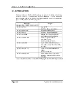


Page: 4-1
AWARD
BIOS SETUP
This chapter shows how to set up the Award BIOS.
Section includes:
z
Introduction
z
Entering Setup
z
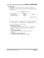
The Standard CMOS Features
z
The Advanced BIOS Features
z
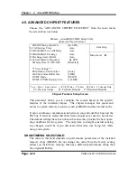
The Advanced Chipset Features
z
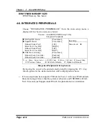
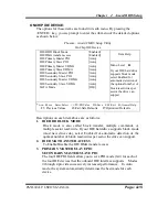
Integrated Peripherals
z
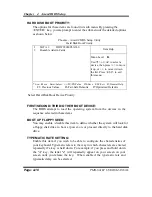
Power Management Setup
z
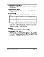
PNP/PCI Configuration
z
PC Health Status
z
Frequency Control
z
Load Fail-Safe Defaults
z
Load Optimized Defaults
z
Password Setting
z
Save and Exit Setup
z
Exit Without Saving
CHAPTER
4


