SE7500CW2 Server Board Technical Product SpecificationSE7500CW2 Connectors and Jumper Blocks
87
Revision 1.40
1.These are “Reserved ” pins on the Intel
®
Xeon processor. In systems utilizing the Intel
®
Xeon processor, the
system designer must terminate these signals to the processor V CC.
2.Baseboards treating AA3 and AB3 as Reserved will operate correctly with a bus clock of 100 MHz.
8.5 System Management Headers
8.5.1
I
2
C Header
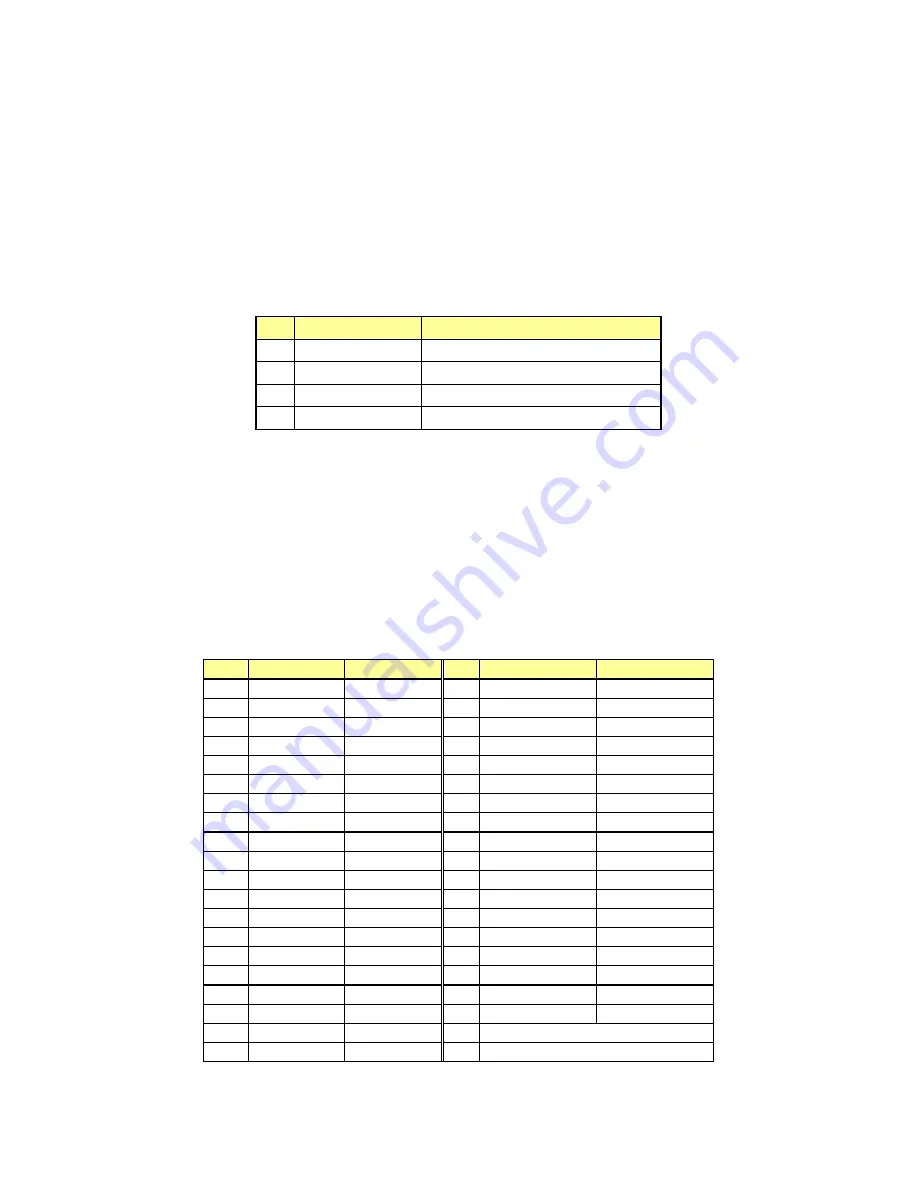
Table 47. SCSI HDD Header Pin-out (J25)
Pin
Signal Name
Description
1
3VSB SDA
Data Line
2
GND
3
3VSB SCL
Clock Line
4
+5VSB
8.6 PCI Slot Connector
There are three PCI buses implemented on the SE7500CW2 board. PCI segment A supports 5V
32-bit/33MHz PCI, segment B supports 3.3V PCI-X 64-bit/100MHz, and segment C supports
3.3V PCI-X 64-bit/133MHz operation. All segments supports full length PCI add-in cards. The pin-
out for each segment is below.
Table 48. P32-A 5V 32-bit/33 MHz PCI Slot Pin-out
Pin
Side B
Side A
Pin
Side B
Side A
1
-12V
TRST#
32
AD[17]
AD[16]
2
TCK
+12V
33
C/BE[2]#
+3.3V
3
Ground
TMS
34
Ground
FRAME#
4
TDO
TDI
35
IRDY#
Ground
5
+5V
+5V
36
+3.3V
TRDY#
6
+5V
INTA#
37
DEVSEL#
Ground
7
INTB#
INTC#
38
Ground
STOP#
8
INTD#
+5V
39
LOCK#
+3.3V
9
PRSNT1#
Reserved
40
PERR#
SMBCLK
10
Reserved
+5V (I/O)
41
+3.3V
SMBDAT
11
PRSNT2#
Reserved
42
SERR#
Ground
12
Ground
Ground
43
+3.3V
PAR
13
Ground
Ground
44
C/BE[1]#
AD[15]
14
Reserved
3.3Vaux
45
AD[14]
+3.3V
15
Ground
RST#
46
Ground
AD[13]
16
CLK
+5V (I/O)
47
AD[12]
AD[11]
17
Ground
GNT#
48
AD[10]
Ground
18
REQ#
Ground
49
Ground
AD[09]
19
+5V (I/O)
PME#
50
CONNECTOR KEY
20
D[31]
AD[30]
51
CONNECTOR KEY


