background image

Product Overview 

Intel® Server Board SE7520BD2 Technical Product Specification 

26  

Revision 

1.3 


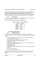
78 AD[49]/CBE[4]# 

Ground 

79 +VI/O 

(3.3V/1.5V) 

AD[48]/CBE[5]# 

80 AD[47] 

AD[46] 

81 AD[45] 

Ground 

82 Ground 

AD[44] 

83 AD[43] 

AD[42] 

84 AD[41] 

+VI/O 

(3.3V/1.5V) 

85 Ground 

AD[40] 

86 AD[39] 

AD[38] 

87 AD[37] 

Ground 

88 +VI/O 

(3.3V/1.5V) 

AD[36] 

89 AD[35] 

AD[34] 

90 AD[33] 

Ground 

91 Ground 

AD[32] 

92 

Riser Presence 1  

Riser Presence 0 

93 Slot2 

REQ Ground 

94 Ground 

Slot2 

GNT 

 
Note:

  The signals in red represent modifications from the standard PCI-X 2.0 pin-out; however, the PCI-X 2.0 

compliant cards can still be used. 

2.9.3 Ultra-320 

SCSI 

Controller 

The Server Board SE7520BD2 provides an embedded dual-channel SCSI bus through the use 
of an LSI* AIC-1030C SCSI controller. The AIC-1030C controller contains two independent 
SCSI controllers that share a single 64-bit/100-MHz PCI-X mode 1 bus master interface as a 
multifunction device, packaged in a 456-pin BGA. Internally, each controller is identical, capable 
of operations using either 16-bit SE or LVD SCS providing 40 MBps (Ultra-wide SE), 80 MBps 
(Ultra 2), 160 MBps (Ultra 160/m) or 320 MBps (Ultra 320/m). Each controller has its own set of 
PCI configuration registers and SCSI I/O registers. The Server Board SE7520BD2 supports 
disabling of the onboard SCSI controller through the BIOS setup menu. 

The Server Board SE7520BD2 provides active terminators, termination voltage, a polyswitch 
fuse, and a protection diode for both SCSI channels. By design, the onboard terminators are 
enabled and no ability is provided to turn off the terminators. The user should plug-in the SCSI 
devices in such a way that the SCSI controller is always at one end of the SCSI bus. This 
provides either RAID 0 (integrated striping) or RAID 1/1e (integrated mirroring/enhanced) 
support.  The array will not span across multiple channels.  All array drives need to be on one 
channel only. 

2.9.4 

Modular RAID on Baseboard (MROMB) 

The Server Board SE7520BD2 baseboard provides the hooks to support Modular RAID on 
Baseboard (MROMB).  

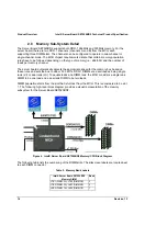
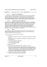
The PCI-X IRQs for slot 2 are PAIRQ<7..4>. During normal operation (no MROMB installed), 
the PAIRQ 6 and 7 are shared between the SCSI device and PCI-X slot 2. When MROMB is 
installed, these interrupts are disconnected from the PXH and used between the SCSI controller 
and the PCI-X slot with the MROMB card. The following diagram outlines the connections on 
the baseboard. 

Summary of Contents for SE7520BD2

Page 1: ...Intel Server Board SE7520BD2 Technical Product Specification C62349 003 Revision 1 3 February 2005 Enterprise Platforms and Services Division ...

Page 2: ...s document contains information on products in the design phase of development Do not finalize a design with this information Revised information will be published when the product is available Verify with your local sales office that you have the latest datasheet before finalizing a design The Intel Server Board SE7520BD2 may contain design defects or errors known as errata which may cause the pr...

Page 3: ...Front Side Bus FSB 9 2 6 3 MCH Memory Sub System Overview 9 2 6 4 PCI Express PCIe 10 2 6 5 Hub Interface 10 2 7 Processor Subsystem Detail 10 2 7 2 Multiple Processor Initialization 12 2 7 3 Processor VRD 12 2 7 4 Reset Configuration Logic 13 2 7 5 Processor Module Presence Detection 13 2 7 6 GTL2006 13 2 7 7 Common Enabling Kit CEK Design Support 13 2 8 Memory Sub System Detail 14 2 8 1 DDR 1 26...

Page 4: ...ds 38 3 2 3 Menu Selection 39 3 2 4 Main Menu 39 3 2 5 Advanced Menu 40 3 2 6 Boot Menu 49 3 2 7 Security menu 51 3 2 8 Server Menu 53 3 2 9 Exit Menu 56 3 3 Other BIOS Configuration Utilities 56 3 3 1 Logo Update Utility 56 3 3 2 Flash Update Utility 56 3 4 Localization Details 57 3 5 Flash Architecture and Flash Update Utility 58 3 5 1 Rolling BIOS and On line Updates 58 3 5 2 Flash Update Utili...

Page 5: ... Alerting 92 4 2 13 NMI Generation 95 4 2 14 SMI Generation 95 4 3 Platform Management Interconnects 95 4 3 1 Power Supply Interface Signals 95 4 3 2 System Reset Control 97 4 3 3 Fan Speed Control 98 4 3 4 Front Panel Control 98 4 3 5 FRU Information 102 4 4 Sensors 102 4 4 1 Sensor Type Codes 102 4 5 Server Management Block Diagram 106 4 6 Management Buses and Connectors 106 4 6 1 SIO Keyboard a...

Page 6: ...3 5 4 3 Logging Format Conventions 124 5 4 4 POST Code Checkpoints 128 5 4 5 Boot Block Initialization Code Checkpoints 130 5 4 6 Boot Block Recovery Code Checkpoint 131 5 4 7 DIM Code Checkpoints 132 5 4 8 Single bit ECC Error Throttling Prevention 132 5 5 Reliability Availability and Serviceability RAS Features 133 5 5 1 Memory RAS features 133 5 5 2 PCI Express 133 5 5 3 RAS Features of FSB 134...

Page 7: ... 7 4 1 Intel SpeedStep Technology 152 7 4 2 Intel Extended Memory 64 Technology 152 7 5 Product Regulatory Compliance 152 7 5 1 Product Safety Compliance 152 7 5 2 Product EMC Compliance 153 7 5 3 Mandatory Standard Certifications Registration Declarations 153 7 5 4 Product Regulatory Compliance Markings 154 7 5 5 Electromagnetic Compatibility Notices 154 7 5 6 Replacing the Back up Battery 154 8 ...

Page 8: ...Board SE7520BD2 V System Block Diagram 8 Figure 6 Intel Server Board SE7520BD2 Memory CPU Block Diagram 14 Figure 7 DIMM Socket Configuration 15 Figure 8 Memory Subsystem 18 Figure 9 MROMB Implementation 27 Figure 10 Block Diagram of Platform Managment Architecture 70 Figure 11 mBMC in a Server Management System 84 Figure 12 External Interfaces to mBMC 86 Figure 13 IPMI over LAN 89 Figure 14 Power...

Page 9: ...per I O Configuration Sub menu 45 Table 19 BIOS Setup USB Configuration Sub menu Selections 45 Table 20 BIOS Setup USB Mass Storage Device Configuration Sub menu Selections 46 Table 21 BIOS Setup PCI Configuration Sub menu Selections 46 Table 22 BIOS Setup Memory Configuration Sub menu Selections 48 Table 23 BIOS Setup Boot Menu Selections 49 Table 24 BIOS Setup Boot Settings Configuration Sub men...

Page 10: ...es and Messages 117 Table 56 Error Codes Sent to Management Module 119 Table 57 POST Error Beep Codes 120 Table 58 Troubleshooting BIOS Beep Codes 120 Table 59 POST Progress Code LED Example 121 Table 60 Memory Error Codes 121 Table 61 Memory Error Events 124 Table 62 Examples of Event Data Field Contents for Memory Errors 125 Table 63 PCI Error Events 126 Table 64 Examples of Event Data Field Con...

Page 11: ...onnector 140 Table 86 PLL Multiplier Selection Bit 0 140 Table 87 PLL Multiplier Selection Bit 1 140 Table 88 Fan 1 and Fan 2 3 Pin 2 Pin 141 Table 89 Fan 3 and Fan 4 141 Table 90 Fan 5 and Fan 6 141 Table 91 BIOS Bank Selection Jumper 142 Table 92 BIOS Recovery Jumper Setting 142 Table 93 Password Clear Jumper Setting 142 Table 94 CMOS Clear Jumper Setting 143 Table 95 Baseboard Power Budget 145 ...

Page 12: ...List of Tables Intel Server Board SE7520BD2 Technical Product Specification xii Revision 1 3 This page intentionally left blank ...

Page 13: ...hitecture is assumed 1 3 Document Outline This document is composed of the following chapters Chapter 1 Introduction Chapter 2 Product Overview Chapter 3 Board Architecture Chapter 4 BIOS Chapter 5 Platform Management Architecture Chapter 6 Error Reporting and Handling Chapter 7 Connector Pin outs and Jumper Blocks Chapter 8 Environmental Specifications Chapter 9 Other Useful Information 1 4 Addit...

Page 14: ...irements of these components when the fully integrated system is used together It is the responsibility of the system integrator that chooses not to use Intel developed server building blocks to consult vendor datasheets and operating parameters to determine the amount of airflow required for their specific application and environmental conditions Intel Corporation cannot be held responsible if co...

Page 15: ...Intel E7520 Memory Controller Hub MCH via Hub Interface 1 5 Supports PXH PCI X bridge interfaced with the MCH via x8 PCI Express PCIe Interface PCI X 2 0 133 MHz slot Two PCI X 1 0 100 MHz slots One PCI Express x8 slot unpopulated on the SE7520BD2 V only One PCI Express x8 actual x4 plumbing to a x8 physical connector slot Marvell Yukon 88E8050 10 100 1000 LAN interfaces with the MCH via x1 PCI Ex...

Page 16: ...rd SE7520BD2 Technical Product Specification 4 Revision 1 3 2 2 Server Board Illustration The following figure provides a high level illustration of the Server Board SE7520BD2 Figure 1 Top Side View of the Intel Server Board SE7520BD2 ...

Page 17: ...ct Specification Product Overview Revision 1 3 Intel Confidential 5 2 3 Mechanical Drawing The following figure provides a mechanical illustration of the Server Board SE7520BD2 Figure 2 Intel Server Board SE7520BD2 Server Board Mechanical Drawing ...

Page 18: ...roduct Specification 6 Revision 1 3 2 4 Server Board Layout Figure 3 illustrates the functional blocks of the Server Board SE7520BD2 as well as the plug in modules that the server board supports Figure 3 Intel Server Board SE7520BD2 SCSI System Block Diagram ...

Page 19: ...Intel Server Board SE7520BD2 Technical Product Specification Product Overview Revision 1 3 Intel Confidential 7 Figure 4 Intel Server Board SE7520BD2 SATA System Block Diagram ...

Page 20: ...nd on the motherboard itself The board part number can also be determined by using Intel Server Management or by checking the System Management Sub menu see Section 3 2 8 1 in BIOS Setup 2 6 Chipset Overview The architecture of the Server Board SE7520BD2 is designed around the Intel E7520 chipset The chipset consists of three components which together are responsible for providing the interface be...

Page 21: ...a base system bus frequency of 200MHz The address and request interface is double pumped at 400MHz while the 64 bit data interface parity is quad pumped to 800MHz This provides a matched system bus address and data bandwidths of 6 4GB sec The newest generation of Intel Xeon processors for dual processor DP servers and workstations is based on the Intel NetBurst microarchitecture These processors f...

Page 22: ...erfaces of the MCH support connection to a variety of bridges and devices compliant with the same revision of the PCI Express Interface Specification Rev 1 0a Refer to the Intel Server Board SE7520BD2 Tested Hardware and OS List for add in cards tested on this platform 2 6 5 Hub Interface The MCH interfaces with the Intel 82801ER I O Controller Hub 5 R ICH5 R via a dedicated Hub Interface supporti...

Page 23: ... can be mixed in a system provided that there is no more than a 1 stepping difference in all processors installed If the installed processors are more than 1 stepping apart an error 8080 through 8183 is logged in the System Event Log SEL and an error 01298000 through 01298003 is reported to the Management Module Acceptable mixed steppings are not reported as errors 2 7 1 2 Mixed Processor Models P...

Page 24: ...uting the BIOS power on self test POST and preparing the machine to boot the operating system At boot time the system is in virtual wire mode and the BSP alone is programmed to accept local interrupts INTR driven by programmable interrupt controller PIC and non maskable interrupt NMI For single processor configurations the system is put in the virtual wire mode which uses the local APIC of the pro...

Page 25: ...llowing circuit is designed to ensure that three criteria are met prior to enabling the embedded VRD Ensure that in a UP configuration the end agent CPU P1 is installed Disable older generation Intel Xeon processors from running in the system to prevent damage to the MCH Ensure in a DP configuration that both processors support the same FSB frequency 2 7 6 GTL2006 The GTL2006 is a 13 bit translato...

Page 26: ...d for the memory bus based on these rules and sets the bus to 266 or 333 MT s DDR 1 DIMMs are described as being single rank s r or dual rank d r To equate loads and DIMM rank the MCH considers a single rank DIMM to be one load and a dual rank DIMM to be two loads DIMM population starts from the slot that is furthest from the MCH This is considered to be slot 1 The following high level block diagr...

Page 27: ...h single dual rank DIMMs the test setups previously listed must be populated according to the following table for each memory channel The test setups assume dual channel operation Empty slots are also noted The maximum memory that can be populated is 16 GB once 4 GB DIMMs are available TSOP DDR333 DIMMs are not supported due to memory timing violations Based on this the Server Board SE7520BD2 and ...

Page 28: ...use the same algorithm but will not have Intel SDDC x4 technology since at most only four bits can be corrected with this ECC The method provides more ECC bits so each ECC word can correct more than a single bit failure This is possible because different mathematical algorithms provide multiple bit correction with the right number of data bits and ECC bits For example a 144 bit ECC word that consi...

Page 29: ...l detect the threshold initiating fail over and escalate the occurrence of that event as directed signal an SMI generate an interrupt or wait to be discovered via polling Whatever software routine responds to the threshold detection must select a victim DIMM in case multiple DIMMs have crossed the threshold prior to sparing invocation and initiate the memory copy Hardware will automatically isolat...

Page 30: ...a cache line of data Interleaved dual channel read to the primary DIMM with even data on channel A Interleaved dual channel read to the mirror DIMM with even data on channel B Non interleaved single channel read pair to channel A with even data on the primary DIMM Non interleaved single channel read pair to channel B with even data on the mirror DIMM When mirroring is enabled via MCH configuration...

Page 31: ...0xA0 DIMM 2B 0xAA DIMM 2A 0xA2 DIMM 1B 0xAC DIMM 1A 0xA4 2 9 PCI Sub System Detail 2 9 1 ICH5 R PCI Interface The Intel 8280 ER I O Controller Hub ICH5 R PCI interface is a multi function device providing an upstream hub interface for access to several embedded I O functions and features including PCI Local Bus Specification Revision 2 3 with support for 33 MHz PCI operations ACPI power management...

Page 32: ...dent SATA signal ports They can be electrically isolated independently Each SATA device can have independent timings They can be configured to the standard primary and secondary channels The Server Board SE7520BD2 supports two SATA connectors for internal HDD supporting RAID The ICH5 SATA RAID has two channels of SATA RAID support It uses the LSI Logic SATA RAID stack which is similar to Intel s R...

Page 33: ... in the previous section the ICH5 R incorporates the Advanced Programmable Interrupt Controller APIC 2 9 1 7 Universal Serial Bus USB Controller The ICH5 R contains an Enhanced Host Controller Interface Specification for Universal Serial Bus Revision 1 0 compliant host controller that supports USB high speed signaling High speed USB 2 0 allows data transfers up to 480 Mb s which is 40 times faster...

Page 34: ...E GPI8 Input Y2 Resume 3 3V WAKE PCI PME GPI9 OC 4 Input B14 Resume 3 3V Reserved for USB OC4 3 in back 2 in front GPI10 OC 5 Input A14 Resume 3 3V PERR for PCI 32bit 33Mhz slot GPI11 SMBALERT Input AC3 Resume 3 3V Board ID 0 GPI12 Input W4 Resume 3 3V SIO SMI GPI13 Input W5 Resume 3 3V BMC IRQ SMI GPI14 OC 6 Input D13 Resume 3 3V SIO ICH5 R PME GPI15 OC 7 Input C13 Resume 3 3V Password clear GPO1...

Page 35: ...ersion 2 0 Quick Command Send Byte Receive Byte Write Byte Word Read Byte Word Process Call Block Read Write and Host Notify 2 9 2 PXH The PXH provides the data interface between the MCH and two PCI X bus segments over a high speed PCI Express x8 link Each of the two PCI segments in the PXH is individually controlled to operate in either PCI or PCI X mode The PXH is configured to support the follo...

Page 36: ...h the slot s modified PCI X 2 0 pin out Table 7 Slot 6 PCI X Pin out Slot 6 PCI X 2 0 Third party Riser Pin Side B Side A 1 12V TRST 2 TCK 12V 3 Ground Riser slot1 clock 4 TDO Riser slot2 clock 5 5V 5V 6 5V INTA 7 INTB INTC 8 INTD 5V 9 PRSNT1 ECC 5 10 ECC 4 VI O 3 3V 1 5V 11 PRSNT2 ECC 3 12 13 CONNECTOR KEYWAY 14 ECC 2 3 3Vaux 15 Ground RST 16 CLK VI O 3 3V 1 5V 17 Ground GNT 18 REQ Ground 19 VI O...

Page 37: ...AD 10 Ground 49 M66EN AD 09 50 Mode 2 Ground 51 Ground Ground 52 AD 08 C BE 0 53 AD 07 3 3V 54 3 3V AD 06 55 AD 05 AD 04 56 AD 03 Ground 57 Ground AD 02 58 AD 01 AD 00 59 VI O 3 3V 1 5V VI O 3 3V 1 5V 60 ACK64 ECC 1 REQ64 ECC 6 61 62 5V KEYWAY KEYWAY 63 Reserved Ground 64 Ground C BE 7 65 C BE 6 CBE 5 AD 48 66 CBE 4 AD 49 VI O 3 3V 1 5V 67 Ground PAR64 ECC 7 68 AD 63 AD 62 69 AD 61 Ground 70 VI O ...

Page 38: ...0 m or 320 MBps Ultra 320 m Each controller has its own set of PCI configuration registers and SCSI I O registers The Server Board SE7520BD2 supports disabling of the onboard SCSI controller through the BIOS setup menu The Server Board SE7520BD2 provides active terminators termination voltage a polyswitch fuse and a protection diode for both SCSI channels By design the onboard terminators are enab...

Page 39: ...K 4 7K PAIRQ 4 INTB PAIRQ 5 PAIRQ 5 Internal to PXH MROMB_IDSEL_N MROMB_PRESENT_N SCSI_INTA SCSI_INTB BE A B C MROMB_IDSEL IDSEL_PA19 Figure 9 MROMB Implementation Table 8 Signal Description Functionality PCI Card Signal Baseboard Signal Description TMS MROMB_IDSEL_N When Asserted disconnects PAA17_N from SCSI controller TDI MROMB_PRESENT_N When Asserted disconnects IRQ s SCSI_INTA and SCSI_INTB f...

Page 40: ...LPC interface 8 16 bit fast X Bus extension for boot flash memory and I O Two sets of BIOS code and data support for main and back up BIOS System health support including LMPC sensor interface fan monitor control and chassis intrusion detection for all configurations i e with or without a BMC or mBMC Serial Interface for manageability Serial Interface M Two to one internally multiplexing of Serial...

Page 41: ... QFN package 2 10 3 1 Intel 82541PI Gigabit Ethernet Controller The Intel 82541PI Gigabit Ethernet controller is a single compact component with an integrated Gigabit Ethernet Media Access Control MAC and physical layer PHY functions The controller allows for Gigabit Ethernet implementation in a very small area It integrates fourth generation gigabit MAC design with fully integrated physical layer...

Page 42: ...rential Buffer The DB800 differential buffer provides 100 MHz reference clocks for the PCI Express devices slots and Serial ATA components The DB800 accepts a single differential clock input from the CK409 clock synthesizer and produces eight buffered differential outputs On the Server Board SE7520BD2 the SRC is connected to the ICH5 R MCH PXH two PCI Express slots and the Marvell Yukon 88E8050 LA...

Page 43: ...firmware interface EFI This is an abstraction layer between the OS and system hardware Server BIOS extensions Provide support for the mini Baseboard Management Controller mBMC and Intelligent Platform Management Interface IPMI Processor Microcode Updates The BIOS also includes the latest processor Microcode updates 3 1 1 Support for BIOS Features ID Feature Name Comments Support at least 128KB of ...

Page 44: ...ump switch support Logging of NMI dump event a Front panel NMI button b OS will log the dump data if NMI button is pressed Power On AC Link When the power returns after failure if it was on it powers back on if it was off it stays off Resume to latest off state Power Switch Disable Power switch can be disabled Power button can be disabled by BIOS setup CPU Memory Failure Continuous operation with ...

Page 45: ...Support for SUP Utility must exist starting at Beta and through production to allow easy updates of BMC HSC FW FRU SDR and BIOS 1 1 Ability to update all SW FW in a single batch process with one reboot at the end of the process 2 Ability to do 1 after booting to a PXE server where the BMC HSC FRU SDR BIOS update files are stored 3 Ability to do 1 after booting locally to a floppy diskette and then...

Page 46: ... hyper threading Enable disable by BIOS setup CPU Micro code update during POST CPU Micro code update during runtime POST runtime Int 15h AX 0D042h Allow variable size microcode update The maximum size of a microcode is 16KB Support for BBS BBS Rev 1 02 Support for PCI PCI X PCI X DDR PCI E Support for MPS APIC mode MPS 1 4 MPS table Support for PIC mode PCI IRQ routing table Support for ACPI a AC...

Page 47: ...er module Sahalee c Subset of IPMI 1 5 for onboard NS PC87431 mBMC Integration with ISM software OS support Microsoft Windows 2003 2000 Linux Novell Security features to protect unwanted tampering of the server ISM provides chassis intrusion and HW and SW change reporting 3 1 2 BIOS Identification String The BIOS Identification string is used to uniquely identify the revision of the BIOS being use...

Page 48: ...0 NIC providing single channel 10 100 1000 3 1 4 BIOS POST The BIOS supports one system splash screen When the system is booting the BIOS displays the splash screen instead of BIOS messages The user can view BIOS messages by pressing the ESC key during POST Once the BIOS POST message screen is selected the splash screen is no longer accessible during the current boot sequence The splash screen can...

Page 49: ...on changes as well as to display current settings and environment information The BIOS Setup stores configuration settings in system non volatile storage Changes effected by BIOS Setup will not take effect until the system is rebooted The BIOS Setup Utility can be accessed from POST by pressing the F2 key Note The BIOS options described in later sections of this document may or may not be present ...

Page 50: ...ed to select the previous value in a pick list or the previous options in a menu item s option list The selected item must then be activated by pressing the Enter key Select Item The down arrow is used to select the next value in a menu item s option list or a value field s pick list The selected item must then be activated by pressing the Enter key Select Menu The left and right arrow keys are us...

Page 51: ...e first screen displayed when entering the BIOS Setup Utility is the Main Menu selection screen This screen displays the major menu selections available The following tables describe the available options on the top level and lower level menus Default values are shown in bold text Table 11 BIOS Setup Main Menu Options Feature Options Help Text Description System Overview AMI BIOS Version N A N A B...

Page 52: ...figure the Floppy drive s Selects submenu Super I O Configuration N A Configure the Super I O Chipset Selects submenu USB Configuration N A Configure the USB support Selects submenu PCI Configuration N A Configure PCI devices Selects submenu Memory Configuration N A Configure memory devices Selects submenu Preproduction Debug N A This option provides engineering access to internal settings It does...

Page 53: ...ading HT Technology in MPS Disabled Enabled Enabling adds secondary processor threads to the MPS Table for pre ACPI OSes Only enable this feature if the pre ACPI OS supports Hyper ThreadingTechnology This option is to support FreeBSD Intel Speed Step Tech Auto Disabled Select disabled for maximum CPU speed Select Auto to allow the OS to reduce power consumption Note This option may not be present ...

Page 54: ...n a given channel Only 1 channel can be S ATA Selects submenu for configuring mixed P ATA and S ATA Primary IDE Master N A While entering setup BIOS auto detects the presence of IDE devices This displays the status of auto detection of IDE devices Selects submenu with additional device details Primary IDE Slave N A While entering setup BIOS auto detects the presence of IDE devices This displays th...

Page 55: ...one Show the second ATA channel configuration The channel will be shown as None if the S ATA_M S ports have already been assigned to first channel Display only If the first channel selects P ATA it reverts to S ATA M S Table 16 BIOS Setup IDE Device Configuration Sub menu Selections Feature Options Help Text Description Primary Secondary Third Fourth IDE Master Slave Device N A N A Display detecte...

Page 56: ... Select DMA Mode Auto Auto detected SWDMA SinglewordDMAn MWDMA MultiwordDMAn UWDMA UltraDMAn The Auto setting should work in most cases S M A R T Auto Disabled Enabled Self Monitoring Analysis and Reporting Technology The Auto setting should work in most cases 32Bit Data Transfer Disabled Enabled Enable Disable 32 bit Data Transfer 3 2 5 3 Floppy Configuration Sub menu Table 17 BIOS Setup Floppy C...

Page 57: ...ration Sub menu Selections Feature Options Help Text Description USB Configuration USB Devices Enabled N A N A List of USB devices detected by BIOS USB Function Disabled Enabled Enables USB HOST controllers When set to disabled other USB options are grayed out Legacy USB Support Disabled Keyboard only Auto Keyboard and Mouse Enables support for legacy USB AUTO option disables legacy support if no ...

Page 58: ...ned by the USB device Emulation Type Auto Floppy Forced FDD Hard Disk CDROM If Auto USB devices less than 530MB will be emulated as Floppy and remaining as hard drive Forced FDD option can be used to force a HDD formatted drive to boot as FDD Ex ZIP drive 3 2 5 6 PCI Configuration Sub menu This sub menu provides control over PCI devices and their option ROM s If the BIOS is reporting POST error 14...

Page 59: ...ration Disabled Enabled Disabled round robin priority scheme for devices on PCI bus Enabled high low priority scheme for devices on PCI bus Round robin verses alternate high low priority scheme In round robin which is default the device with the lowest req gnt pair gets first chance at the bus In this case the baseboard devices have an advantage reg gnt 0 followed by the bottom slots req gnt 1 mid...

Page 60: ...ystem Memory Settings DIMM 1A Installed Not Installed Disabled Mirror Spare Informational display DIMM 1B Installed Not Installed Disabled Mirror Spare Informational display DIMM 2A Installed Not Installed Disabled Mirror Spare Informational display DIMM 2B Installed Not Installed Disabled Mirror Spare Informational display DIMM 3A Installed Not Installed Disabled Mirror Spare Informational displa...

Page 61: ...o replace failures Mirroring keeps a second copy of memory contents Sparing or Mirroring is grayed out if the installed DIMM configuration does not support it 3 2 6 Boot Menu Table 23 BIOS Setup Boot Menu Selections Feature Options Help Text Description Boot Settings Boot Settings Configuration N A Configure settings during system boot Selects submenu Boot Device Priority N A Specifies the boot de...

Page 62: ... Displays Press F2 to run Setup in POST Scan User Flash Area Disabled Enabled Allows BIOS to scan the Flash ROM for user binaries 3 2 6 2 Boot Device Priority Sub menu Selections Table 25 BIOS Setup Boot Device Priority Sub menu Selections Feature Options Help Text Description Boot Device Priority 1st Boot Device Varies Specifies the boot sequence from the available devices A device enclosed in pa...

Page 63: ...he available devices Varies based on system configuration 3 2 7 Security menu Table 29 BIOS Setup Security Menu Options Feature Options Help Text Description Security Settings Administrator Password is N A Install Not installed Informational display User Password is N A Install Not installed Informational display Set Admin Password N A Set or clear Admin password Pressing enter twice will clear th...

Page 64: ... until a password is entered A password is required to boot from a diskette This node is grayed out if a user password is not installed Diskette Write Protect Disabled Enabled Disable diskette write protection when Secure mode is activated A password is required to unlock the system This node is grayed out if a user password is not installed This node is hidden if the Intel Management Module is no...

Page 65: ... restored Power On boots the system after power is restored Last State is only displayed if the Intel Management Module is present When displayed Last State is the default When set to Stays Off Power Switch Inhibit is disabled FRB 2 Policy Disable BSP Do not disable BSP Retry on Next Boot Disable FRB2 Timer This controls action if the boot processor will be disabled or not Disable BSP and Do not d...

Page 66: ...art Number N A N A Field content varies System Serial Number N A N A Field content varies Chassis Part Number N A N A Field content varies Chassis Serial Number N A N A Field content varies BIOS Version N A N A BIOS ID string excluding the build time and date BMC Device ID N A N A Field content varies BMC Firmware Revision N A N A Field content varies BMC Device Revision N A N A Field content vari...

Page 67: ...dware Carrier Detect for modem use Terminal Type PC ANSI VT100 VT UTF8 VT100 selection only works for English as the selected language VT UTF8 uses Unicode PC ANSI is the standard PC type terminal ACPI Redirection Disabled Enabled Enable Disable the ACPI OS Headless Console Redirection Serial Port Connector Serial A Serial B Selects which serial port will be routed to the serial port connector on ...

Page 68: ...hanges and Exit N A Exit system setup without saving any changes ESC key can be used for this operation Discard Changes N A Discards changes done so far to any of the setup questions F7 key can be used for this operation Load Setup Defaults N A Load Setup Default values for all the setup questions F9 key can be used for this operation Load Custom Defaults N A Load custom defaults Save Custom Defau...

Page 69: ...fbb bat depending upon whether the boot block needs to be updated 7 f bat Updates system ROM only boot block does not change 8 fbb bat Updates both system ROM and the boot block 9 Note If running fbb bat or f bat the J1B1 jumper BIOS partition selection should be set to pins 1 2 to select the correct BIOS partition 10 When the Flash Update is complete a message will appear on the screen indicating...

Page 70: ...fers to the capability of having two copies of BIOS the current one in use and a second BIOS to which an updated BIOS version can be written When ready the system can roll forward to the new BIOS In case of a failure with the new version the system can roll back to the previous version The BIOS relies on specialized hardware and additional flash space to accomplish online update rolling of the BIO...

Page 71: ...troy System CMOS r registry path to store result of operation only for Windows version k Program non critical block only not supported s Leave signature in BIOS q Silent execution h Print help 3 5 2 2 Updating the BIOS from DOS Make sure that the flash bootable disk contains both the ROM image and the afudos update utility Boot to DOS Run the afudos utility as follows AFUDOS i ROM filename n p b n...

Page 72: ...updated independent of the system BIOS The command line usage for the UbinD utility is as follows UBinD R or I or D M ModID F RomFileName B NewUserBinaryFileName N NewRomFileName O NCB R replaces the user binary module I inserts the user binary module D deletes the user binary module from the ROM file displays help information M ModID is hexadecimal user binary module ID Default ModID 0xF0 O NCB i...

Page 73: ...e it is recommended that the OEM modify the provided AMIBOOT ROM file with the user binary or OEM logo tools before performing the recovery A BIOS recovery can be accomplished from one of the following devices a standard 1 44 or 2 88 MB floppy drive an USB Disk On Key an ATAPI CD ROM DVD an ATAPI ZIP drive or a LS 120 LS 240 removable drive The recovery media must include the BIOS image file AMIBO...

Page 74: ...has been read the system will increment the file extension and then begin searching for the next file If searching for the AMIBOOT 002 file the system will beep 2 times each beep 1sec long with a 0 5 sec gap between beeps If searching for the AMIBOOT 003 file the system will beep three times with a 0 5 sec gap between beeps This process would continue until the total file size read in is equal to ...

Page 75: ...exe file is NOT the same for both DOS and Microsoft Windows 98 2000 XP The user must use the correct Rombuild exe file dependent upon whether he or she is updating the OEM logo in DOS or in a Microsoft Windows 98 2000 XP environment 3 6 OEM Binary System customers can supply 16 KB of code and data for use during POST and at run time Individual platforms may support a larger user binary User binary...

Page 76: ...d has only the advantage that it does not use up limited option ROM space and more option ROMs space can be used for other devices If user binary code is required at run time it is copied to the option ROM space At each scan point during POST the system BIOS determines if the scan point has a corresponding user binary entry point to transfer control to To determine this the bitmap at byte 4 of the...

Page 77: ...n instruction db 04h Bit map to define call points a 1 in any bit specifies that the BIOS is called at that scan point in POST db CBh First transfer address used to point to user binary extension structure dw Word Pointer to extension structure dw 0 Reserved This is a list of 7 transfer addresses one for each bit in the bitmap 5 Bytes must be used for each JMP ErrRet JMP ErrRet JMP Start JMP to ma...

Page 78: ...nters or leaves a sleep state The following table describes the type of checkpoints that may occur during ACPI sleep or wake events Table 35 ACPI Runtime Checkpoints Checkpoint Description AC First ASL check point Indicates the system is running in ACPI mode AA System is running in APIC mode 01 02 03 04 05 Entering sleep state S1 S2 S3 S4 or S5 10 20 30 40 50 Waking from sleep state S1 S2 S3 S4 or...

Page 79: ...tionally installed Flexible Management Module FMM that plugs into a dedicated server management connector on the baseboard When an FMM is installed the mBMC is automatically converted from an autonomous controller to an I2 C based I O device allowing the Sahalee BMC to completely manage the system Tier 3 Advanced Optional Like the Standard management model the Advanced management model is implemen...

Page 80: ...g No Yes Yes Wake On Ring WOR support No Yes Yes Access via web browser No No Yes SNMP access No No Yes Telnet access No No Yes Alerting via Email No No Yes Keyboard Video Mouse KVM redirection via LAN No No Yes High speed access to dedicated NIC No No Yes Table 37 Power and Reset Control Power Cycle Power Up Power Down Hard Reset Source Ess Std Adv Ess Std Adv Ess Std Adv Ess Std Adv DPC Serial N...

Page 81: ...otected No Action Unprotected Protected No Action Unprotected Unprotected Essentials S4 S5 Off Protected No Action Unprotected Protected No Action Unprotected Unprotected Table 39 Memory RAS Feature Support by Server Management Tier Memory RAS Feature Essentials Standard Advanced Inventory No Yes Yes Correctable Error Reporting No Yes Yes Uncorrectable Error Reporting Yes Yes Yes DIMM Sparing Part...

Page 82: ...H SMBus I2C 1 FMM Connector Mini BMC SDR FRU SEL I2 C 2 DIMM6 DIMM5 DIMM4 DIMM3 DIMM2 DIMM1 PWR_GOOD Power Control Power Control FRU PS1 PS1 FRU PS2 PS2 FRU FMM Present IPMB POWER UNIT Figure 10 Block Diagram of Platform Managment Architecture 4 1 2 5V Standby The power supply must provide a 5V Standby power source for the platform to provide any management functionality 5V Standby is a low power ...

Page 83: ...in interpreting and presenting sensor data Together IPMI Messaging and the SDRs provide a self descriptive abstracted platform interface that allows management software to automatically configure itself to the number and types of platform management features on the system In turn this enables one piece of management software to be used on multiple systems Since the same IPMI messages are used over...

Page 84: ... events The baseboard monitoring can be extended by implementing an IPMI compatible management controller connecting it to the IPMB and adding new SDRs describing that controller and its sensors to the SDR Repository System Management Software can then read the SDRs and use them to automatically incorporate the additional sensors 4 1 5 Private Management Buses A Private Management Bus is a single ...

Page 85: ...e used by BIOS and run time management software as a way to detect software hangs The management controller provides out of band remote management interfaces providing access to the platform health event log and recovery control features via LAN all tiers Standard and Advanced systems also allow access via serial modem IPMB PCI SMBus and ICMB interfaces These interfaces remain active on standby po...

Page 86: ...for enabling add in cards to access the baseboard management subsystem Standard and Advanced systems only Watchdog Timer with selectable timeout actions power off power cycle reset or NMI and automatic logging of timeout event Direct Platform Control DPC LAN Remote Management Connection LAN Alerting via PET Platform Event Trap format SNMP trap Serial Modem Remote Management Connection Standard and...

Page 87: ...able 40 mBMC Built in Sensors Sensor Name Sensor Sensor Type Event Reading Type Event Offset Triggers Assert Deassert Readable Value Offsets EventData Physical Security Violation 01 Physical Security 05h Sensor Specific 6Fh LAN Leash Lost As LAN Leash Lost Trig Offset Platform Security Violation 02 Platform Security Violation Attempt 06h Sensor Specific 6Fh Out of band access password violation As...

Page 88: ... Threshold 01h u l c nc As De Analog R T Fault LED Action 01 BB 5V 0Fh Voltage 02h Threshold 01h u l c nc As De Analog R T Fault LED Action 01 BB 12V 10h Voltage 02h Threshold 01h u l c nc As De Analog R T Fault LED Action 01 BB 12V 11h Voltage 02h Threshold 01h u l c nc As De Analog R T Fault LED Action 01 Aux 3 3V 12h Voltage 02h Threshold 01h u l c nc As De Analog R T Fault LED Action 01 STBY 5...

Page 89: ...LED Action 02 Proc2 Thermal trip 24h Processor 07h Sensor Specific 6Fh Thermal Trip As Trig Offset Fault LED Action 02 Proc1 Thermal Control 25h Temp 01h Threshold 01h u c nc As De Analog Trig Offset Fault LED Action 01 Proc2 Thermal Control 26h Temp 01h Threshold 01h u c nc As De Analog Trig Offset Fault LED Action 01 Diagnostic Interrupt Button 27h Critical Interrupt 13h Sensor Specific 6Fh FP N...

Page 90: ...s from redund Non red Suff res from insuff res Non red Insuff res Redundancy Degraded from full redundancy Redundancy Degraded from non redundant As Trig Offset A X Watchdog 03h Watchdog2 23h Sensor Specific 6Fh Timer Expired Hard Reset Power Down Power Cycle Timer Interrupt As De Trig Offset A X Platform Security Violation 04h Platform Security Violation Attempt 06h Sensor Specific 6Fh Secure mod...

Page 91: ... De Analog R T A BB 1 8V SCSI Core 13h Voltage 02h Threshold 01h u l nr c nc As De Analog R T A BB 2 5V 14h Voltage 02h Threshold 01h u l nr c nc As De Analog R T A BB 3 3V 15h Voltage 02h Threshold 01h u l nr c nc As De Analog R T A BB 3 3V Standby 16h Voltage 02h Threshold 01h u l nr c nc As De Analog R T A X BB 3 3V AUX 17h Voltage 02h Threshold 01h u l nr c nc As De Analog R T A X BB 5V 18h Vo...

Page 92: ...Ch Slot Connector 21h Sensor Specific 6Fh Device Installed As De Trig Offset A Fan 3 Presence 4Dh Slot Connector 21h Sensor Specific 6Fh Device Installed As De Trig Offset A Fan 4 Presence 4Eh Slot Connector 21h Sensor Specific 6Fh Device Installed As De Trig Offset A Fan Redundancy 4Fh Fan 04h Generic 0Bh Redundancy Regained Redundancy lost Redundancy Degraded Non red Suff res from redund Non red...

Page 93: ...ower Gauge aggregate power Power Supply 1 7Ch Other Units 0Bh Threshold 01h u l nr c nc As De Analog R T A Power Gauge aggregate power Power Supply 2 7Dh Other Units 0Bh Threshold 01h u l nr c nc As De Analog R T A Processor Missing 80h Module Board 15h Digital Discrete 03h State Asserted State Deasserted As Trig Offset A System ACPI Power State 82h System ACPI Power State 22h Sensor Specific 6Fh ...

Page 94: ... Non red Suff res from insuff res Non red Insuff res As Trig Offset A Memory Mirroring Enabled 8Ch Entity Presence 25h Sensor Specific 6Fh Entity Present As Trig Offset A Processor 1 Status 90h Processor 07h Sensor Specific 6Fh IERR Thermal Trip FRB1 FRB2 FRB3 Config Error Presence Disabled As De Trig Offset M X Processor 2 Status 91h Processor 07h Sensor Specific 6Fh IERR Thermal Trip FRB1 FRB2 F...

Page 95: ...et M Processor 1 Vcc D0h Voltage 02h Threshold 01h u l nr c nc As De Analog R T A Processor 2 Vcc D1h Voltage 02h Threshold 01h u l nr c nc As De Analog R T A CPU Configuration Error D8h Processor 07h Generic 03h State Asserted As De Discrete R T A DIMM 1 E0h Slot Connector 21h Sensor Specific 6Fh Fault Status Asserted Device Installed Disabled As Trig Offset A DIMM 2 E1h Slot Connector 21h Sensor...

Page 96: ...ing the system monitoring the sensors and communicating with other systems and devices via various external interfaces The following figure is a block diagram of the mBMC as it is used in a server management system The external interface blocks to the mBMC are the discrete hardware peripheral device interface modules Figure 11 mBMC in a Server Management System SMBus mBMC Bus Interface Uni SMBus G...

Page 97: ...he mBMC interfaces with the host through the slave SMBus interface It interfaces with the LAN On Motherboard LOM and peripherals through the two independent master bus interfaces 4 2 4 External Interface to mBMC Figure 12 shows the data control flow to and within the functional modules of the mBMC External interfaces from the host system LOM and peripherals interact with the mBMC through the corre...

Page 98: ...gents must use the mBMC Master Write Read I2 C command if they require direct communication with a device on this bus In addition the mBMC provides a Reserve Device command that gives an external agent exclusive access to a specific device for a selectable time 4 2 5 Messaging Interfaces This section describes the supported mBMC communication interfaces Host SMS interface via SMBus interface LAN i...

Page 99: ...the mBMC via the System Management Bus SMBus The interface consists of three signals SMBus clock signal SCLH SMBus data signal SDAH Optional SMBus alert signal SMBAH The signal notifies the host that the PC87431x has data to provide The mBMC is a slave device on the bus The host interface is designed to support polled operations Host applications can optionally handle an SMBus alert interrupt if t...

Page 100: ...g in the form of SNMP traps that conform to the IPMI Platform Event Trap PET format Table 44 LAN Channel Capacity LAN CHANNEL Capability Options Number of Sessions 1 Number of Users 1 User Name NULL anonymous User Password Configurable Privilege Levels User Operator Administrator Authentication Types MD5 Number of LAN Alert Destinations 1 Address Resolution Protocol ARP Gratuitous ARP 4 2 6 Direct...

Page 101: ...rly the management controller can use the side band interface to send packets from Port 26Fh as shown in the following figure LAN PCI NIC 1 mBMC System Bus RMCP Port 26Fh In band Traffic side band connection Figure 13 IPMI over LAN RMCP includes a field that indicates the class of messages that can be embedded in an RMCP message packet For RMCP version 1 0 the defined classes are IPMI ASF and OEM ...

Page 102: ...river or NIC configuration is used it is possible to get driver timeouts when the IPMI over LAN feature is enabled 4 2 6 3 BIOS Boot Flags A remote console application can use the IPMI Set System Boot Options command to configure a set of BIOS boot flags and boot initiator parameters that are held by the management controller These parameters include information that identifies the party that init...

Page 103: ...on 1 5 The SEL is accessible via all communication transports In this way the SEL information can be accessed while the system is down by means of out of band interfaces The maximum SEL size that is supported by mBMC is 92 entries Supported commands are Get SEL Info Reserve SEL Get SEL Entry Add SEL Entry Clear SEL Get SEL Time Set SEL Time 4 2 9 1 SEL Erasure TBD 4 2 9 2 Timestamp Clock The mBMC ...

Page 104: ...Repository Erasure TBD 4 2 10 2 Initialization Agent The mBMC implements the internal sensor initialization agent functionality specified in the Intelligent Platform Management Interface Specification Version 1 5 When the mBMC initializes or when the system boots the initialization agent scans the SDR repository and configures the sensors referenced by the SDRs This includes setting sensor thresho...

Page 105: ...ned in the following table Note An action that has changed from delayed to non delayed or an action whose delay time has been reduced has a higher priority Each generated event is logged to the SEL Table 46 PEF Action Priorities Action Priority Delayed Type Note Power down 1 Yes PEF Action Soft shut down 2 Yes OEM PEF Action Not executed if a power down action was also selected Power cycle 3 Yes P...

Page 106: ...e Alert over LAN feature is used to send either Platform Event Trap alerts or directed events to a remote system management application regardless of the state of the host s operating system LAN alerts may be sent over the LAN channel LAN alerts can be used by PEF to send out alerts to selected destination whenever an event matches an event filter table entry For more information on LAN alerts see...

Page 107: ...eceiving a Chassis Control command issued from one of the command interfaces Use of this command will not cause an event to be logged in the SEL Detecting that the front panel Diagnostic Interrupt button has been pressed A PEF table entry matching an event where the filter entry has the NMI action indicated A processor IERR or Thermal Trip if the mBMC is so configured Watchdog timer pre timeout ex...

Page 108: ...er If AC power is suddenly lost the mBMC 1 Immediately asserts system reset 2 Powers down the system 3 Waits for configured system off time depending on configuration 4 Attempts to power the system on depending on configuration 4 3 1 1 Power up Sequence When turning on the system power in response to one of the event occurrences listed in Table 48 the mBMC executes the following procedure 1 The mB...

Page 109: ...r power cycle 3 Platform Event Filtering PEF Turns power OFF or power cycle 4 Command Routed through command processor Turns power ON or OFF or power cycle 5 Power state retention Implemented via mBMC internal logic Turns power ON when AC power returns 6 Chipset sleep S5 Turns power ON or OFF 4 3 2 System Reset Control 4 3 2 1 Reset Signal Output The mBMC asserts the System Reset signal on the bas...

Page 110: ... at which the Fan Speed increases does not correspond to a non critical warning condition for the fan because the fan s state is still OK from the system s point of view The baseboard has two analog Fan Speed signals that are driven by pulse width modulator PWM circuits by the baseboard hardware These signals can be driven to several levels according to temperature measurements Multiple bytes of a...

Page 111: ...rough the front panel connector to the mBMC which monitors and de bounces it The signal must be stable for at least 25ms before a state change is recognized An assertion of the front Panel Reset signal to the mBMC causes the mBMC to start the reset and reboot process This action is immediate and without the cooperation of any software or operating system running on the system If Secure Mode is ena...

Page 112: ...t timeout for the command is 15 seconds The baseboard supports the optional command parameter to allow the timeout to be set anywhere from 1 to 255 seconds The optional timeout parameter in the Chassis Identify command also allows software to tell the LED to go Off immediately The Chassis Identify Pushbutton works using a push on push off operation Each press of the push button toggles the LED sig...

Page 113: ...he Chassis Intrusion signal and makes the status of the signal available via the Get Chassis Status command and Physical Security sensor state If enabled a chassis intrusion state change causes the mBMC to generate a Physical Security sensor event message with a General Chassis Intrusion offset 4 3 4 7 Front Panel Lockout The management controller monitors a Secure Mode signal from the keyboard co...

Page 114: ...e accessed using IPMI Master Write Read commands 4 3 5 1 mBMC FRU Inventory Area Format The mBMC FRU inventory area format follows the Platform Management FRU Information Storage Definition Refer to Platform Management FRU Information Storage Definition Version 1 0 for details The mBMC provides only low level access to the FRU inventory area storage It does not validate or interpret the data store...

Page 115: ...ffsets for discrete sensors that are readable via the Get Sensor Reading command Unless otherwise indicated all Event Triggers are readable i e Readable Offsets consists of the reading type offsets that do not generate events Event Data This is the data that is included in an event message generated by the associated sensor For threshold based sensors the following abbreviations are used R Reading...

Page 116: ...Data PEF Action SDR Record Type Physical Security Violation 07h Physical Security 05h Sensor Specific 6Fh General Chassis Intrusion As General Chassis Intrusion Trig Offset X 02 CPU1 12v 08h Voltage 02h Threshold 01h u l nr c nc As De Analog R T Fault LED Action 01 CPU2 12v 09h Voltage 02h Threshold 01h u l nr c nc As De Analog R T Fault LED Action 01 BB 1 5V 0Ah Voltage 02h Threshold 01h u l nr c...

Page 117: ...As De Analog R T Fault LED Action 01 Tach Fan 6 1Ah Fan 04h Threshold 01h u l nr c nc As De Analog R T Fault LED Action 01 Tach Fan 7 1Bh Fan 04h Threshold 01h u l nr c nc As De Analog R T Fault LED Action 01 Tach Fan 8 1Ch Fan 04h Threshold 01h u l nr c nc As De Analog R T Fault LED Action 01 Tach Fan 9 1Dh Fan 04h Threshold 01h u l nr c nc As De Analog R T Fault LED Action 01 System Event 1Eh Sy...

Page 118: ...old 01h u l nr c nc As De Analog R T Fault LED Action 01 Proc1 Core temp 29h Temp 01h Threshold 01h u l nr c nc As De Analog R T Fault LED Action 01 Proc2 Core temp 2Ah Temp 01h Threshold 01h u l nr c nc As De Analog R T Fault LED Action 01 CPU Configuration Error 2Bh Processor 07h Generic 03h State Asserted As De Discrete R T Fault LED Action 02 4 5 Server Management Block Diagram 4 6 Management ...

Page 119: ...ctor are typically pulled up to 5V and the KVM solution is not 5V tolerant Voltage translation logic is available on the module to convert the bi directional interface to a signaling level the KVM solution can tolerate In order for the KVM solution to work the PS2 to SIO connection on the baseboard must be broken Logic must be supplied on the baseboard to break the connection when the KM_INHIB_N s...

Page 120: ...face system management mode interface and the ACPI embedded controller interface The KCS interface 0 has the ability to interrupt the host by assertion of the SYSIRQ output The KCS ports provided by the FMM reside at specific I O addresses on the host s LPC bus These addresses are programmable by firmware running on the FMM to provide for system integration flexibility Externally these ports are a...

Page 121: ...lave addresses The I2 C clock and data inputs to the Sahalee are digitally filtered so that input glitches of less than four Sahalee clock cycles are rejected Both high and low polarity glitches are rejected This specification defines a transaction as a data transfer bounded by a START and STOP or bounded by a START and repeated START A stream is defined as one or more transactions bounded by a ST...

Page 122: ...nt at 2 8 V output buffers 4 6 10 Sleep States Supported The ICH5 R controls the system sleep states States S0 S1 S4 and S5 are supported Either the BIOS or an operating system invokes the sleep states This is done in response to a power button being pressed or an inactivity timer countdown Normally the operating system determines which sleep state to transition into However a 4 second power butto...

Page 123: ...tem up from any sleep state except mechanical off 4 6 11 1 Wake from S1 Sleep State During S1 the system is fully powered permitting support for wake on USB wake on PS2 keyboard mouse wake on RTC Alarm and wake on PCI PME wake on USB wake on PS2 keyboard mouse and wake on RTC Alarm are not supported by POE BIOS 4 6 11 2 Wake from S4 and S5 States Power button and LAN events are used to wake from S...

Page 124: ...s for PWR SLP HDD and other LEDs as specified in SSI EEB are supported on the front panel header A dual color LED can be used for the PWR SLP LED to distinguish between System Power On Green and System Sleep Yellow The PWR SLP LED signals are driven by the ICH and conditioned by logic on the baseboard before they are sent to the front panel connector The single HDD LED represents any hard drive ac...

Page 125: ...hassis An Identification Switch An Identification LED Additionally the front panel has a built in temperature sensor DS1621 that communicates via the SMB port at Address 9A While the Server Board SE7520BD2 complies with SSI EEB the front panel does implement all of the recommended features in SSI EEB and adds some additional features not covered in the specification Figure 15 Front Panel Pinout O ...

Page 126: ...fication Identification OFF No Identification Requirements To support the front panel connectivity a 2x17 0 1 inch pitch non shrouded polarized header is required The first 24 pins 2x12 follow the SSI EEB Specification for pin out definition and functionality Pins 25 26 of the header are not installed to allow a 2x12 connector as specified in the SSI EEB to plug in LED power can be supplied to the...

Page 127: ...RB3 timer is set by system firmware 5 2 2 FRB 2 BSP POST Failures The second timer FRB 2 is set to several minutes by BIOS and is designed to guarantee that the system completes POST The FRB 2 timer is enabled just before the FRB 3 timer is disabled to prevent any unprotected window of time Near the end of POST the BIOS disables the FRB 2 timer If the system contains more than 1 GB of memory and t...

Page 128: ...on functional If the BIOS detects that an AP has failed BIST or is non functional it requests the BMC to disable that processor Processors disabled by the BMC are not available for use by the BIOS or the OS Since the processors are unavailable they are not listed in any configuration tables including the SMBIOS tables 5 2 6 Treatment of Failed Processors All failures FRB 3 FRB 2 FRB 1 and AP failu...

Page 129: ...e as the operation field represents the specific initialization activity Based upon the data bit availability to display a progress code progress codes can be customized to fit the data width The higher the data bit the higher the granularity of information Progress codes may be reported by either the system BIOS or option ROMs The Response section in the following table is divided into three diff...

Page 130: ...nt stepping Pause 0192 L2 cache size mismatch Pause 0193 CPUID Processor stepping are different Pause 0194 CPUID Processor family are different Pause 0195 Front side bus mismatch System halted Pause 0196 CPUID Processor Model are different Pause 0197 Processor speeds mismatched Pause 5120 CMOS Cleared By Jumper Warning 8103 Warning Unsupported USB device found and disabled Warning 8104 Warning Por...

Page 131: ...eed mismatch detected 00019700 Processor P0 failed BIST 00019701 Processor P1 failed BIST 00150100 Multi bit error occurred forcing NMI DIMM 00150100 Multi bit error occurred forcing NMI DIMM DIMM could not isolate 289 DIMM D is Disabled 00150900 SERR PERR Detected on PCI bus no source found 00151100 MCA Recoverable Error Detected Proc 00151200 MCA Unrecoverable Error Detected Proc 00151300 MCA Ex...

Page 132: ...add in card 8 If the system video adapter is an add in card replace or reseat the video adapter If the video adapter is an integrated part of the system board the board may be faulty 5 3 3 Checkpoints 5 3 3 1 System ROM BIOS POST Task Test Point Port 80h Code The BIOS will send a 1 byte hex code to the port 80 before each task The port 80 codes provide a troubleshooting method in the event of a sy...

Page 133: ... 1 1 0 0 0 Result Amber Green Red Off MSB LSB 5 3 3 2 Memory Error Codes In table 60 below these memory errors are written at POST and in the SEL Table 60 Memory Error Codes Tpoint Description 001h MEM_ERR_CHANNEL_B_OFF DIMM mismatch forced Channel B disabled 002h MEM_ERR_CK_PAIR_OFF Slow DIMM s forced clock pair disabled 0E1h MEM_ERR_NO_DEVICE No memory installed 0E2h MEM_ERR_TYPE_MISMATCH 0E3h M...

Page 134: ... appropriate key before booting the OS or entering BIOS Setup 5 4 Error Logging 5 4 1 Error Sources and Types One of the major requirements of server management is to correctly and consistently handle system errors System errors can be categorized as follows PCI bus Memory single and multi bit errors Sensors Processor internal errors bus address errors thermal trip errors temperatures and voltages...

Page 135: ...tection capabilities of the processors by setting appropriate bits in the processor model specific register MSR and appropriate bits inside the chipset In the case of irrecoverable errors on the host processor bus proper execution of the SMI handler cannot be guaranteed and the SMI handler cannot be relied upon to log such conditions The BIOS SMI handler will record the error to the SEL only if th...

Page 136: ... Event Data 2 and Event Data 3 for memory errors PCI bus errors and FRB 2 errors is described in the following three tables This format is supported by all platforms that are IPMI version 1 0 or later compliant Bits 3 1 of the generator ID field define the format revision The system software ID is a 7 bit quantity For events covered in this document the system software ID will be within the range ...

Page 137: ...cified According to Table 30 3 in IPMI_1 3 0 is 0 for single bit error and 1 for multi bit error Event Data 2 7 0 OEM code 2 or unspecified For format rev 0 if this byte is specified 7 6 Zero based Memory card number Matches the number of Type 16 entry in SMBIOS table For example card 0 corresponds to the first Type 16 entry in SMBIOS tables If all DIMMs are onboard this field will always be 0 5 0...

Page 138: ...his document 3 0 Offset from Event Trigger for discrete event state Follow IPMI definition If either of the two data bytes following this do not have any data that byte should be set to 0xff and the appropriate filed in event data 1 should indicate that that it is unspecified According to Table 30 3 in IPMI_1 3 0 is 04 for PCI PERR and 05 for PCI SERR Event Data 2 7 0 OEM code 2 or unspecified For...

Page 139: ...code in byte 2 5 4 00 unspecified byte 3 10 OEM code in byte 3 BIOS will not use encodings 01 and 11 for errors covered by this document 3 0 Offset from Event Trigger for discrete event state If Event data 2 and event data 3 contain OEM codes bits 7 6 and bits 5 4 contain 10 For platforms that do not include the POST code information with FRB 2 log both these fields will be 0 BIOS either should sp...

Page 140: ...Initializes the CPU The BAT test is being done on KBC Program the keyboard controller command byte is being done after Auto detection of KB MS using AMI KB 5 C0 R R OFF OFF Early CPU Init Start Disable Cache Init Local APIC C1 R R OFF G Set up boot strap processor Information C2 R R G OFF Set up boot strap processor for POST C5 R A OFF G Enumerate and set up application processors C6 R A G OFF Re ...

Page 141: ...e memory 60 OFF R R OFF Initializes NUM LOCK status and programs the KBD typematic rate 75 OFF A R A Initialize Int 13 and prepare for IPL detection 78 G R R R Initializes IPL devices controlled by BIOS and option ROMs 7A G R A R Initializes remaining option ROMs 7C G A R R Generate and write contents of ESCD in NVRam 84 R G OFF OFF Log errors encountered during POST 85 R G OFF G Display errors to...

Page 142: ... detection Execute full memory sizing module Verify that flat mode is enabled D3 R R G A If memory sizing module not executed start memory refresh and do memory sizing in Boot block code Do additional chipset initialization Re enable CACHE Verify that flat mode is enabled D4 R A OFF R Test base 512KB memory Adjust policies and cache first 8MB Set stack D5 R A OFF A Boot block code is copied from R...

Page 143: ... checkpoint E9 EF A A A G Read error occurred on media Jump back to checkpoint EB F0 R R R R Search for pre defined recovery file name in root directory F1 R R R A Recovery file not found F2 R R A R Start reading FAT table and analyze FAT to find the clusters occupied by the recovery file F3 R R A A Start reading the recovery file cluster by cluster F5 R A R A Disable L1 cache FA A R A R Check the...

Page 144: ... onboard peripherals that are set to an automatic configuration and configures all remaining PnP and PCI devices 5 4 8 Single bit ECC Error Throttling Prevention The system detects corrects and logs correctable errors As long as these errors occur infrequently the system should continue to operate without a problem Occasionally correctable errors are caused by a persistent failure of a single comp...

Page 145: ... sparing The MCH included specialized hardware to support fail over to a spare DIMM device in the event that a primary DIMM in use exceeds a specified threshold of runtime errors This prevents a failing DIMM with increasing error frequency from causing a catastrophic failure This feature is an alternative to memory mirroring 5 5 1 3 DDR 1 Memory Mirroring The mirroring feature is fundamentally a w...

Page 146: ...rther data protection is provided as illegal codes can be detected 5 5 3 RAS Features of FSB The FSB incorporates parity protection for the data pins of the FSB There is no ECC for FSB signals 5 5 4 PCI X PCI X provides two signals for detection and signaling of two kinds of errors This includes data parity and system errors The first of these is PERR parity error reporting which is used for signa...

Page 147: ...ower is available and required to be less than 200mA 5 5 5 4 Inputs The POWER_OFF signal is an input to turn off DC power to the unit It is passed to the system as if a front panel power button had been pressed Pulse width must be greater than 16ms for ICH debounce circuitry The PCIRST signal is an input to reset the system It is passed to the system as if a front panel reset button had been press...

Page 148: ...Shrouded Header 40 SCSI LED 2 Header 4 Fans 8 Header 3 Battery 1 Battery Holder 3 Power supply 3 EPS12V Power 8 24 5 Keyboard Mouse 1 PS2 stacked 12 Rear USB 1 External Stacked 12 Serial Port 1 External D Sub 9 Video connector 1 External D Sub 15 Dual LAN connector 10 100 1000 1 Dual LAN connector with in built magnetic 38 Floppy drive 1 Header 34 Front panel main 1 Header 34 Front panel USB 1 Hea...

Page 149: ... on peripheral bus will cease master transactions This is a GPO from ICH and will be a high of 3 3V It is assumed this meets the VIH of the OEM input buffer This is an active high signal and when this signal is low the OEM RMC card should not be issuing any transactions on the SMBus PCIRST 6 Input from RMC card This is fed into a 5V tolerant AND gate that logically ORs the front panel reset button...

Page 150: ...y IDE Connector Signal Name Pin Pin Signal Name IDE_RST_N 1 2 GND ICH5_PDD7 3 4 ICH5_PDD8 ICH5_PDD6 5 6 ICH5_PDD9 ICH5_PDD5 7 8 ICH5_PDD10 ICH5_PDD4 9 10 ICH5_PDD11 ICH5_PDD3 11 12 ICH5_PDD12 ICH5_PDD2 13 14 ICH5_PDD13 ICH5_PDD1 15 16 ICH5_PDD14 ICH5_PDD0 17 18 ICH5_PDD15 GND 19 20 KEY ICH5_PDDREQ 21 22 GND ICH5_PDIOW_N 23 24 GND ICH5_PDIOR_N 25 26 GND ICH5_PDIORDY 27 28 GND CSEL ICH5_PDDACK_N 29 ...

Page 151: ... ICH5_SMBCLK FP_SLPBTN_N 19 20 FP_CHASSIS_INTRUDER_N GND 21 22 NICB_ACT_LED_N FP_NMI_BTN_N 23 24 NICB_LINK_LED_N KEY 25 26 KEY P5V_STBY 27 28 P5V_STBY FP_ID_LED_N 29 30 FP_SYS_READY_LED_N FP_ID_BTN_N 31 32 TP_FP_CONN_32 GND 33 34 DPP_FAULT_LED_N Table 80 USB Front Connector Signal Name Pin Pin Signal Name USB_PWR 1 2 Not Used USB_ICH5_P0N_IND 3 4 Not Used USB_ICH5_P0P_IND 5 6 Not Used GND 7 8 Not ...

Page 152: ...S ATA0_TX_P 5 S ATA0_TX_N 6 GND 7 Table 83 Battery Holder Signal Name Pin VBAT 1 VBAT 2 GND 3 Table 84 Piezo Speaker Signal Name Pin SPEAKER_OUT 1 GND 2 Table 85 SCSI LED Connector Signal Name Pin GND 1 SCSI_CONN_LED_N 2 SCSI_CONN_LED_N 3 GND 4 Table 86 PLL Multiplier Selection Bit 0 Signal Name Pin MCH_PLLSEL0 1 GND 2 Table 87 PLL Multiplier Selection Bit 1 Signal Name Pin MCH_PLLSEL1 1 GND 2 ...

Page 153: ...1 3 Intel Confidential 141 Table 88 Fan 1 and Fan 2 3 Pin 2 Pin Signal Name Pin Ground 1 Fan Power 2 Fan Tach 3 Signal Name Pin Fan LED 1 Fan Presence 2 Table 89 Fan 3 and Fan 4 Fan LED 1 Fan Presence 2 PWM 3 Ground 4 Fan Power 5 Fan Tach 6 Table 90 Fan 5 and Fan 6 Signal Name Pin PWM 1 Ground 2 Fan Power 3 ...

Page 154: ...der offers two possible positions jumper on or jumper off Jumper on indicates a Flash Recovery and jumper off indicates normal operation Table 92 BIOS Recovery Jumper Setting Jumper Description Setting J4H1 Recovery Operation Jumper On Recovery operation Jumper Off Normal boot default 6 2 3 Password Clear If the User or Administrator password s is lost or forgotten both passwords may be cleared by...

Page 155: ...ting Jumper Description Setting J2H1 CMOS Clear 1 2 CMOS Clear by BMC default 2 3 CMOS Clear Force Erase Procedure of CMOS Clear by BMC Push power botton to power off and then pressed the reset botton continually then push the power botton once Figure 16 Jumper Locations U ATA 100 Primary Floppy BATTERY J1B1 Rolling BIOS Bank J2H1 CMOS Clear J4H1 BIOS Recovery J4H3 Password Clear ...

Page 156: ...ecifications and Cooling Requirements Non operating temperature requirements From 40 degrees C to 70 degrees C Operating temperature requirements From 5 degrees C to 50 degrees C Voltage tolerance of all system power supply rails 5 Cooling requirements for various areas of board CPU and CPU VR 450LFM DIMM memory array TBD MCH heat sink TBD PXH heat sink TBD ...

Page 157: ... Utilize Factor Average Power 5 V 3 3 V 12 V 12VCPU 12 V 5 V 5VSB Jayhawk Processor Vcore 2 204 00 21 25 Processor VRD Eff 80 20 51 00 VTT 1 2V 3 5A 70 2 94 0 98 NB Lindenhurst Vcc Core 1 5V 5 11A 1 70 5 37 1 34 Vcc DDR 2 5V 10W 1 70 7 00 0 73 1 5 V VRD Eff 80 20 1 34 2 5 V VRD Eff 80 20 3 85 ICH5 V_CPU_IO 0 0025 A 70 0 0020 0 0002 0 0002 Vcore 1 5V 0 971A 70 0 38 0 25489 VCC3 3V 0 480 A 70 0 50 0...

Page 158: ...1PI 3 3V 025A 1 8V 21A 1 2V 45A 70 0 70 0 480 88E8050 1 70 1 33 0 266 VGA ATI_RAGE_XL 1 70 2 10 0 420 0 07 Super I O W83627HF VCC 5V 0 02A 1 70 0 70 0 14 VCC3 3V 015 A 1 70 0 03 0 011 VSB5V 01 A 1 70 0 04 0 01 SCSI LSI1030 1 3 3V 1A LP3963 70 2 31 0 58 1 8V 1 8A 1587 70 2 27 0 859 CLK3 3 CY28329 Generator 1 70 0 81 0 245 Video RAM 2MX 32 1 70 0 69 0 210 System ROM FWH 1 70 0 03 0 008 mBMC AUX5V 1 ...

Page 159: ...ntial 147 CPU Fan 2 100 38 40 0 48 PCI 32 Bit 5V 1 40 10 00 2 00 2 280 0 40 0 20 0 375 PCI X 100 3 3V 2 40 20 00 4 00 4 560 0 40 0 040 PCI X 266 1 5V 133 3 3V 1 40 10 00 2 00 2 280 0 40 0 020 PCI EXPRESS 3 3V 2 60 30 00 6 000 2 94 0 30 0 040 Board Level Power 511 Board Level output current 13 8 18 3 15 1 21 3 0 5 1 9 ...

Page 160: ...P3V3_STBY Linear Regulator from 5V Standby 2 5 3 3V Auxiliary P3V3_AUX Switches between 3 3V main and standby power rail depending on normal operation and sleep states respectively 3 1 2V P_VTT Linear Regulator from 1 8V 3 1 5V P1V5 Switching Regulator from 5V 3 1 8V P1V8_SCSI Linear Regulator from 3 3V 3 2 5V P2V5_VIDEO Linear Regulator from 5V 3 2 5V PV_SCSIA PV_SCSIB Linear Regulator from 5V 1 ...

Page 161: ...will be required if the Heceta 7 is NOT available for power ON There is a 1msec delay from the VTT_PWRGD generated from the P_VTT 1 2V regulator power good signal to the SB_VTT_PWRGD which is used for generating the VID_PWRGD for the CPUs Similarly there is a 1msec delay from the time the SB_VTT_PWRGD is generated to VR0_SYS_ENABLE These details are not shown in the following diagram This delay lo...

Page 162: ... Diagram The Power Good signal from the power supply starts the reset sequence in the system The intent of the power good signal and the reset sequence is to ensure that all components are held in reset mode until power and system clocks have stabilized The power good signal from the power supply will go true after all the output voltages have reached specified levels Power Good will go false just...

Page 163: ... P3V3 N12V P_VTT PS_PWR_GD P1V8_SCSI P1V5 AC Plug In 2 5S max 5mS to 400mS Wait for PS_ON_N 100mS min 1Sec Max When all are good Time not to scale P3V3_STBY P1 8V_NIC P1V0_NIC 1mS max 10mS max 1mS to 20mS 1mS to 20mS P1V8 P_VCCP0 P_VCCP1 10mS max 1mS to 20mS If CPU1 Present 1mS max P3V3_AUX_SWITCH P3V3_AUX 1mS max P1V5_PXH Figure 18 Intel Server Board SE7520BD2 Power Sequencing Diagram ...

Page 164: ...ete with a demonstrated 32 656 hours Since our current validation test is only run up to about 32 000 hours across multiple servers we still maintain that actual MTBF data will likely be over 102 000 hours of operation based on statistical regression 7 4 1 Intel SpeedStep Technology Intel Xeon processors support the Geyserville3 GV3 feature of Intel SpeedStep Technology This feature changes the pr...

Page 165: ...ZS 3548 Class A Emissions Australia New Zealand BSMI CNS13438 Class A Emissions Taiwan DOC GOST R 29216 91 Class A Emissions Russia 1 GOST R 50628 95 Immunity Russia 1 RRL MIC Notice No 1997 41 EMC and 1997 42 EMI Korea Note 1 Certifications for boards in Russia and Belarus are not legal requirements however for ease of importing boards into these countries the boards must be listed on a System le...

Page 166: ...has been marked with the C Tick Mark to illustrate its compliance 7 5 5 3 Ministry of Economic Development New Zealand Declaration of Conformity This product has been tested to AS NZS 3548 and complies with New Zealand Ministry of Economic Development emission requirements 7 5 5 4 BSMI Taiwan The BSMI Certification number R33025 is silk screened on the component side of the server board and the fo...

Page 167: ...batteri Eksplosjonsfare Ved utskifting benyttes kun batteri som anbefalt av apparatfabrikanten Brukt batteri returneres apparatleverandøren VARNING Explosionsfara vid felaktigt batteribyte Använd samma batterityp eller en ekvivalent typ som rekommenderas av apparattillverkaren Kassera använt batteri enligt fabrikantens instruktion VAROITUS Paristo voi räjähtää jos se on virheellisesti asennettu Va...

Page 168: ...on Intel Server Board SE7520BD2 Technical Product Specification 156 Intel Confidential Revision 1 3 8 Other Useful Information 8 1 Platform Confidence Test PCT See the system board Resource CD The executable is named BYOPCT ...

Page 169: ...00 7 Fixed Front side bus sequence mismatch warning message with P03 BIOS 8 Fixed Under Microsoft Windows 2003 and Microsoft Windows 2000 OS cannot recognize 6 Gigabytes of memory 9 No Fix Onboard CTRL C RAID 0 1 creation appears to be slow and limit the number of RAID configurations 10 No Fix Two Monitors appear in Microsoft Windows 2003 device manager 11 Fixed Wrong front panel identification in...

Page 170: ...led to disable a timer before expiration Intel found that this false error message is caused by the onboard platform instrumentation not consistently recognizing the BIOS command to disable the timer This anomaly is present on the server boards with FRU SDR version BD 6 2 1 and prior Currently the Intel Server Board SE7520BD2 is shipping with FRU SDR version 6 2 1 pre installed from Intel s factor...

Page 171: ...ror please reboot the system Implication Configuring the Zero Channel RAID ZCR is impossible Workaround The Intel RAID Contoller SRCZCRX ZCR is fully supported Refer to the Tested Hardware and Operating System List rev1 60 on http support intel com support motherboards server se7520bd2 sb CS 013538 htm for full support details on the Intel equivalent card Status Fixed with BIOS P05 00 5 Intel Xeon...

Page 172: ...on the Intel support website to fix this issue see URL below Please use the inf posted on the support intel com website for Microsoft Windows 2003 and all of the chassis products Microsoft Windows 2000 Backplane Driver WIN2K_HSBP_INF_FILE EXE First level reference http support intel com support motherboards server chassis SC5200 Second level reference http downloadfinder intel com scripts df Detai...

Page 173: ... Windows Server 2003 Enterprise fastdetect pae C Microsoft Windows Status The workaround specified above is the only fix 9 Onboard CTRL C RAID 0 1 creation appears to be slow and limit the number of RAID configurations Problem When building a low level RAID 0 1 mirror configuration it appears to be very slow and never complete Also there appears to be a limitation on how many RAID devices a channe...

Page 174: ...ther one will be listed as the Plug and Play Monitor This issue is not caused by the IMM module but by the ATI VGA chip OPROM and will not be fixed because ATI has no plans to resolve it Implication A user may be confused when operating with only one monitor why two show up in the Windows device manager The second monitor is necessary for the Keyboard Video Mouse KVM feature of the Advanced Intel ...

Page 175: ...ess Red Hat develops the driver to support this function 13 Boxboard Configuration Label has incorrect SSI Front Panel Connector pin out Problem Boxboard Configuration Label has incorrect SSI Front Panel Connector pin out Please see Table 79 in this document for the correct pin out definition Implication The wrong configuration label may confuse some channel customers Workaround Intel Server Board...

Page 176: ... label C71061 005 Intel Server Board SE7520BD2V C76556 005 and below will be fixed in WW10 with C76556 006 and with label C71901 005 Status Intel will fix this problem with new labels 15 System fault LED glowing continuously Fab605 board Problem The onboard system fault LED continuously glows on the Fab605 board Implication Customers may feel that the LED is working abnormally and that the board m...

Page 177: ...efinition ACPI Advanced Configuration and Power Interface BMC Baseboard Management Controller CEK Common Enabling Kit DVI Digital Video Interface FML Fast Management Link FMM Firmware management module FSB Front Side Bus KCS LPC Low Pin Count mBMC Mini Baseboard Management Controller MCH Memory Controller Hub NMI Non maskable Interrupt PATA Parallel ATA PCB Printed Circuit Board PLL Phase Lock Loo...

Page 178: ...ec htm Server Power Control White Paper Revision 0 93 November 5 1998 Intel Corporation The SMBus Specification Intel Corporation Processor Intel Netburst Micro Architecture BIOS Writer s Guide Confidential Document OR 2445 Prescott Intel Xeon and Potomac Processor BIOS Writer s Guide Confidential Document 13579 Application Note AP 485 Intel Processor Identification and the CPUID Function http www...

Page 179: ...m PC2001 System Design Guide http www pcdesguide com PCI Local Bus Specification Revision 2 2 http www pcisig org PCI to PCI Bridge Specification Revision 1 1 http www pcisig org PCI BIOS Specification Revision 2 1 http www pcisig org PCI Power Management Specification Revision 1 0 http www pcisig org PCI IRQ Routing Table Specification Revision 1 0 Microsoft Corporation POST Memory Manager Specif...

Reviews: