Developer’s Manual
January, 2004
141
Intel XScale® Core
Developer’s Manual
Software Debug
9.11.2
DBGTX JTAG Register
The ‘DBGTX’ JTAG instruction selects the DBGTX JTAG data register. The JTAG opcode for this
instruction is ‘0b0010000’. The debug handler uses the DBGTX data register to send data to the
debugger. A protocol can be setup between the debugger and debug handler to allow the debug handler
to signal an entry into debug mode, and once in debug mode to transmit data requested by the debugger.
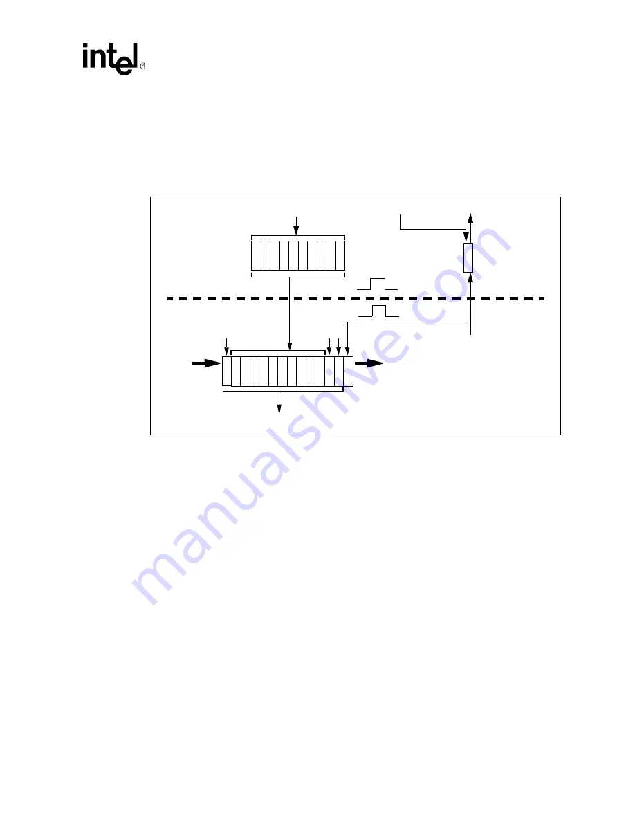
A Capture_DR loads the TX register value into DBG_SR[34:3] and TXRXCTRL.TR into
DBG_SR[0]. The other bits in DBG_SR are loaded as shown in
Figure 9-1
.
The captured TX value is scanned out during the Shift_DR state. Transitioning from Shift_DR
immediately to Capture_DR after capturing a ‘1’ in DBG_SR[0] automatically clears TXRXCTRL.TR.
Data scanned in is ignored on an Update_DR.
9.11.2.1
DBG_SR[0]
DBG_SR[0] is used for part of the synchronization that occurs between the debugger and debug
handler for accessing TX. The debugger polls DBG_SR[0] to determine when the TX register
contains valid data from the debug handler.
A ‘1’ captured in DBG_SR[0] indicates the captured TX data is valid. After capturing valid data, the
debugger must place the JTAG state machine in the Shift_DR state to guarantee that a debugger read
clears TXRXCTRL.TR. A ‘0’ indicates there is no new data from the debug handler in the TX register.
9.11.2.2
TX (DBG_SR[34:3])
DBG_SR[34:3] is updated with the contents of the TX register following an Update_DR.
Note:
If DBG_SR[0] is ‘0’ following an Update_DR, the contents of DBG_SR[34:3] are unpredictable.
Figure 9-2.
DBGTX
TDO
TDI
DBG_SR
Capture_DR
Update_DR
1
2
3
34
35
0
31
TXRXCTRL
TX
Core CLK
software read-only
0
0
0
1
28
set by SW write to TX
cleared by Debugger read
Ignored
software write
TCLK