SECTION 7
System Information
PEN*KEY
R
6200/6300 Hand-Held Computer Programmer’s Reference Guide 7-17
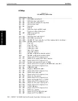
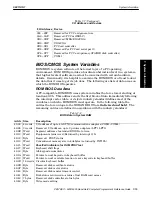
Table 7Ć8 (Continued)
BIOS Data in System RAM
Addr
Description
Size
40:A1 39 bytes Reserved
40:C8 10 bytes Reserved for real mode restart stackĊ
used by RESTART
40:D2 Word
RSĆ232 timeout counterĊused by interrupt 14h
40:D4 4 bytes
ReservedĊ
used by POST
40:D8 20 words ReservedĊ
for NORAND BIOS
CMOS Registers
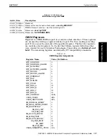
Registers in CMOS RAM are part of a realĆtime clock interface. These registers
are accessed by writing a register number to port 70h, then reading or writing
port 71h to access the contents of the specified register. The first few registers
are realĆtime clock registers. In the list that follows, register definitions that
were created for use by Intermec Technologies Corporation are
italicized and
bold
. The remaining registers are defined by PC compatibility standards.
Table 7Ć9
CMOS Register Assignments
Register Name
Value Definition
RTC_SECONDS
0
RTC_SECONDS_ALARM
1
RTC_MINUTES2
RTC_MINUTES_ALARM
3
RTC_HOURS4
RTC_HOURS_ALARM
5
RTC_WEEKDAY
6
RTC_DAY
7
RTC_MONTH
8
RTC_YEAR
9
RTC_REG_A
10
RTC_REG_B
11
RTC_REG_C
12
RTC_REG_D
13
RTC_CENTURY
032h
CMOS_DIAGS
0Eh
CMOS_SHUTDOWN
0Fh
SD_NORMAL_RESET
0
SD_REAL_MODE_ENTRY
1
SD_BOOTSTRAP
4
SD_EOI_JMP
5
SD_FAR_JMP
6
SD_BLOCK_MOVE1
7
SD_MEM_TEST
8
SD_BLOCK_MOVE2
9
SD_FAR_JMP2
10
SD_IRET
11
SD_FAR_RET
12
CMOS_DISKETTE1_TYPE
10h
7. System Information

