


Application Note 1655
2
AN1655.0
August 18, 2011
remote sensing, RM+2, RM-2 need to be changed to higher
values, such as 10
Ω
.
To assess stability, RM+2 can be changed to a 100
Ω
resistor,
then inject the signal across VSEN+ and VSEN_PRIME.
JP201 is a SIP connector that can be used with R223 = 0
Ω
installed to inject a clock signal to synchronize the module to.
The default phase shift of the CLKOUT signal from the module
causes a second module to switch with a phase shift of 180°.
This can be demonstrated on the 2-phase evaluation board,
ISL8200MEVAL2PHZ.
R203 and C210 are small added filters for the VIN pins.
The Overcurrent Protection (OCP) limit can be controlled by
shorting the jumper marked FIXED and populating a resistor in
R209A’s location, as per your desired OCP trip point. As another
option, by shorting the jumper marked ADJ1, you can tune the
OCP level using the potentiometer labeled R241. To measure the
resistance of R241, simply turn off the part and remove the short
across ADJ1 and place a resistance meter across it’s terminals.
If the application is in the 3.3V range, tie VIN and PVCC to 5.0V.
However, in applications that involve a PVIN greater than 5.5V,
open the jumper named PVIN, not doing so will increase the
probability of tying VCC to a voltage greater than its capability.
Shorting the jumper marked VCC will allow you to use a separate
power supply for VCC; however this is not a necessity as VCC can
be internally generated within the module.
Evaluating Other Output
Voltages
The ISL8200MEVAL1PHZ kit has several preset outputs for
convenience. 1.2V, 1.5V, 1.8V, 2.5V, 3.3V and 5.0V can be easily
selected by shorting their appropriate jumper. There is also a
potentiometer provided that will allow for any other output
voltage between 0.6V to 6V. Equation 1 governs the relationship
between the VSET resistors (R221A thru R221F) and the output
voltage.
The output capacitors (C9 and C19) must be changed to support
the corresponding output voltage. The onboard output capacitors
are rated at 2V max.
Programming the Input Voltage
UVLO and its Hysteresis
By modifying the voltage divider at the EN pin connected to the
input rail (R1 and R2), the input UVLO and its hysteresis can be
programmed. The ISL8200MEVAL1PHZ evaluation board comes
stocked with R1 = 8.25k
Ω
and R2 = 3.01k
Ω
; this sets the UVLO
level at 2.9V for a 3.3V application.
For a 5V application, with a UVLO at 4V and recover at 4.5V, use
R1 = 16.6k
Ω
and R2 = 4.2k
Ω
. The UVLO equations are re-stated
in the following, where R1 and R2 are the upper and lower
resistors of the voltage divider at the EN pin respectively, V
HYS
is
the desired UVLO hysteresis and V
FTH
is the desired UVLO falling
threshold; a user selected value. Equation 2 describes V
HYS
as
the point past the programmed UVLO level at which the device
turns on again.
For example, in a 5V application where it is desired to have the
part turn off at 4V and recover at 4.5V, the V
HYS
that goes in
Equation 3 is 0.5V.
For 12V applications, if it is desired to have the IC disabled when
the input voltage drops below 9V and restart when V
IN
recovers
above 10.6V, then R1 = 53.33k
Ω
and R2 = 5.2k
Ω
.
Efficiency Measurement
The voltage and current meter can be used to measure
input/output voltage and current. In order to obtain an accurate
measurement and prevent the voltage drop of PCB or wire trace,
the voltage meter must be close to the input/output terminals.
For simplicity, the measuring point for the input voltage meter is
at the PVIN_TP terminal, and the measuring point for the output
voltage meter is at the TP310 terminal.
The efficiency equation is shown in Equation 5:
Output Ripple/Noise
Measurement
Simple steps should be taken to ensure that there is minimum
pickup noise due to high frequency events, which can be
magnified by the large ground loop formed by the oscilloscope-
probe ground. This means that even a few inches of ground wire
on the oscilloscope probe may result in hundreds of millivolts of
noise spikes when improperly routed or terminated. This effect
can be overcome by using the short loop measurement method
to minimize the measurement loop area for reducing the pickup
noise. The short loop measurement method is shown in Figure 2.
R221X
V
OUT
V
REF
–
(
)
V
REF
(
)
-------------------------------------
ROS
=
where V
REF
= 0.6V
ROS = 2.2k
Ω
internal
(EQ. 1)
UVLO
TURN ON
–
V
HYS
V
FTH
+
=
(EQ. 2)
R1
V
HYS
I
HYS
-------------
=
I
HYS
= N x 30µA
N = number of phases
(EQ. 3)
R2
R
1
V
ENREF
⋅
V
FTH
V
ENREF
–
---------------------------------------
=
V
ENREF
= 0.8V
(EQ. 4)
Efficiency
Output Power
Input Power
-----------------------------------
P
OUT
P
IN
-------------
V
OUT
I
OUT
•
(
)
V
IN
I
IN
•
(
)
-----------------------------------
=
=
=
(EQ. 5)
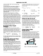
FIGURE 2. OUTPUT RIPPLE/NOISE MEASUREMENT
OUTPUT CAP
OR MOSFET
OUTPUT CAP
OR MOSFET
OUTPUT CAP


