


UG105 Rev.0.00
Page 4 of 14
Aug 14, 2017
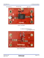
ISL8215MEVAL1Z
2. Functional Description
2.
Functional Description
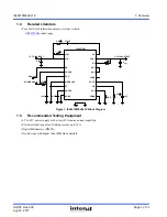
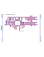
The ISL8215MEVAL1Z provides the peripheral circuitry to evaluate the feature set of the ISL8215M. The evaluation
board is designed with mechanical switches for ENABLE, several connectors, test points, and jumpers, which makes
validation of the module easy. The converter can be enabled and disabled by toggling the ENABLE switch as shown in
Figure 2 on page 6
. Connecting a jumper across the pins as shown in
Figure 2
enables the PSM/DEM mode of
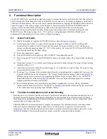
operation, which can lead to higher efficiencies at light loads. Selecting features like external frequency
synchronization can be performed by hooking the signal generator (square pulse waveform clock signal) to the
MOD/SYNC pin. The output voltage (0.6V - 12V) and the switching frequency (300kHz to 2MHz) can be
programmed by changing the resistors as shown in
Figure 3 on page 6
.
2.1
Quick Test Guide
(1) Disable the module by toggling the ENABLE switch as shown in
Figure 2 on page 6
.
(2) Use the appropriate cables to connect the DC input power supply to banana sockets J1 and J4 and the
electronic load to sockets J3 and J2. Ensure that the polarity for the power leads is correct and the input
voltage is within the operating range (7V - 42V) of the module. Use test points TP1 (VIN) and TP2 (PGND)
for accurately measuring the input voltage.
(3) Turn on the input power supply.
(4) Turn the ENABLE switch to position “SW1 ENABLE” for enabling the module.
(5) Probe test points TP3 (VOUT) and TP4 (PGND) to observe the output voltage. The output voltage should read
3.3V.
(6) Adjust input voltage, V
IN
, within the specified range and observe output voltage. The output voltage variation
should be within ±1.5%.
(7) Adjust the load current to within the specified range (0 - 15A) and observe output voltage. The output voltage
variation should be within ±1.5%.
(8) To change V
OUT
, disconnect the evaluation board from the setup and populate a standard 0603 resistor at the
R
2
placeholder location on the bottom layer. The “Output Voltage Resistor Settings” table in the
ISL8215M
datasheet can be used as a reference for programming different output voltages. Refer to the “ISL8215M
Design Guide Matrix” table in the
ISL8215M
datasheet for correct input and output capacitors, switching
frequency, and output voltage combinations.
(9) The switching frequency can be modified by populating a standard 0603 resistor at the R
11
placeholder
location on the bottom layer. Refer to “Equation 2” in the
ISL8215M
datasheet for selecting the correct value
of R
11
within admissible operating range (300kHz - 2MHz).
2.2
Thermal Considerations and Current Derating
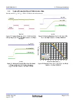
Board layout is very critical so that the module can operate safely and deliver the maximum allowable power. For
the board to operate properly at high ambient temperature environments and carry full load current, the board
layout needs to be carefully designed to maximize thermal performance. To achieve this, use enough trace width,
copper weight, and proper connectors.
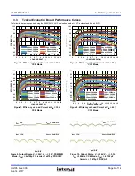
The ISL8215MEVAL1Z evaluation board is capable of operating at 15A full load current at room temperature
without the need for additional cooling systems. However, if the board is to operate at elevated ambient
temperatures, then the available output current may need to be derated. Refer to the derated current curves in the
ISL8215M
datasheet to determine the maximum output current the evaluation board can supply.
Summary of Contents for ISL8215MEVAL1Z
Page 14: ...ISL8215MEVAL1Z UG105 ...


