


UG105 Rev.0.00
Page 5 of 14
Aug 14, 2017
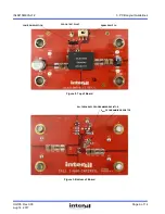
ISL8215MEVAL1Z
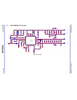
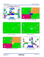
3. PCB Layout Guidelines
3.
PCB Layout Guidelines
The ISL8215MEVAL1Z evaluation board is a 1.8inx3in four-layer FR-4 board with 2oz. copper on all the layers. The
board can be used as a single 15A reference design. Refer to
Figures 15
through
20
for board layout information.
The ISL8215MEVAL1Z board layout has been optimized for electrical performance, low loss, and good thermal
performance. Similar performance can be obtained for designs involving ISL8215M, while adhering to the following
layout design tips:
3.1
Layout Considerations
(1) The input capacitors and high frequency decoupling ceramic capacitors are placed between VIN and PGND,
as close to the module as possible. The loop formed by the input capacitor, VIN pad, and PGND is kept as
small as possible, to minimize the high frequency noise. The output capacitors are placed closer towards the
load. Short, wide copper planes are used to connect the output capacitors to the load for avoiding any parasitic
inductances and resistances.
(2) Large copper planes are used for VIN, VOUT, and PGND to minimize conduction loss and thermal stress.
Multiple vias are used to connect the power planes in different layers.
(3) Ground planes are used in the internal layers (Layer 2 and Layer 3) with shared SGND and PGND to simplify
the layout design. The controller SGND has a solid connection to the PGND through multiple vias. The
bottom layer is used to route EN and VCC signals. PGOOD is routed on the top layer.
(4) For achieving a tight output voltage regulation, the V
OUT+
point is connected to the Remote Sense (RS) pin by
routing the trace through inner Layer 3. A 2Ω resistor is placed close to the RS pin for damping the noise on
the traces.
(5) To avoid ground bouncing issues, place the V
IN
return and the V
OUT
return diagonally opposite to each other.
This ensures that the switching noise generated by the power-train will have a minimal effect on the controller
operation.
(6) Because the phase nodes are subjected to very high dv/dt voltages, the parasitic capacitor formed between
these islands and the surrounding circuitry will tend to couple the switching noise. The PHASE node is placed
in Layer 3 and the bottom layer of the PCB to minimize its impact on the operation of the controller. The
sensitive signal traces (EN, VCC, and PGOOD) are routed away from the PHASE node plane to minimize
noise coupling.
(7) The VCC bypass capacitor is placed underneath the VCC pin, and its ground is connected to the PGND pad.
The low-side feedback resistor, R
2
, and the decoupling capacitor, C
25
, are connected to the SGND pad through
multiple vias.
(8) For a switching frequency of 300kHz, a 4.02Ω 1206 resistor and a 270pF 100V X7R 0603 capacitor in series
from PH to VIN is required. De-rate the resistor size for switching frequencies higher than 300kHz. Calculate
the power dissipated in resistor (P
cal
) by using the formula C • V
2
• f, where,
• C = 270pF
• V = Input voltage
• f = Frequency of operation.
For derating purposes, the nominal power handling capability of the resistor package size should be at least
P
cal
/0.65. The 65% derating is derived by looking at the resistor operation at +100°C ambient temperature.
Use a standard thick film chip resistor datasheet to find the correct resistor package size for different switching
frequencies and input voltage.
Summary of Contents for ISL8215MEVAL1Z
Page 14: ...ISL8215MEVAL1Z UG105 ...


