Open-Q™ 845 µSOM Development Kit User Guide
Version 1.0
© Copyright Intrinsyc Technologies Corporation
26 of 30
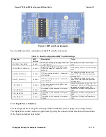
If the user intends to use a mini-PCIe card on the dev kit that requires a USB connection, then the
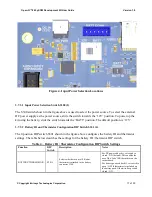
Mini-PCIe USB enable DIP switch S2401 (6) must be switched to closed / ON. See Figure 6. Mini-
PCIe USB Enable DIP Switch (6). If the DIP switch is closed, the USB 3.1 Type A connector J2400
(5) is not functional.
3.7.16
Digital IO Expansion Header J2200 (23)
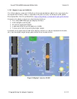
The Open-Q 845 µSOM Development Kit includes a digital IO expansion header J2200 which
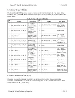
provides access to a selection of µSOM GPIO signals and power rails. See item 23 in Figure 1 for
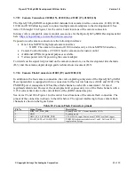
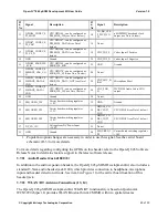
the carrier board location of this header. The pinout for this header is shown in the table below.
Table 11. Digital IO Expansion Header J2200 Pinout
Pin
No
Signal
Description
Pin
No
Signal
Description
1
VREG_S4A_1P8
µSOM LDO Regulator
S4A +1.8V
2
VREG_S4A_1P8
µSOM LDO Regulator S4A
+1.8V
3
SSC8_QUP2_0_SPI2_
MISO
CPU Sensor Core
SSC_GPIO8
4
MB_VREG_3P3
Carrier board switching
regulator. 3.3V
5
SSC9_QUP2_1_SPI2_
MOSI
CPU Sensor Core
SSC_GPIO9
6
GPIO11_LCD_TE1
CPU GPIO11
7
SSC10_QUP2_2_SPI2
_CLK
CPU Sensor Core
SSC_GPIO10
8
GPIO0_QUP0_L0_SPI
_MISO
CPU GPIO0
9
SSC11_QUP2_3_SPI2
_CS_N
CPU Sensor Core
SSC_GPIO11
10
GPIO1_QUP0_L1_SPI
_MOSI
CPU GPIO1
11
GND
Ground
12
GPIO2_QUP0_L2_SPI
_CLK
CPU GPIO2
13
GPIO56_QUP10_1_I2
C_SCL
CPU GPIO56
14
GPIO3_QUP0_L3_SPI
_CS_N
CPU GPIO3
15
GPIO55_QUP10_0_I2
C_SDA
CPU GPIO55
16
GPIO7_LCD1_RST_N
CPU GPIO7
17
GND
Ground
18
GND
Ground
19
No Net
20
MB_VREG_5P0
Carrier board switching
reg5.0V
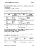
For more details regarding configuring the GPIOs on this header, refer to the Open-Q 845 Software
Release Notes to determine feature support in the latest software release.
3.7.17
Sensor IO Expansion Header J2100 (21)
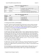
The Open-Q 845 µSOM Development Kit includes a sensor expansion header J2100 which provides
a connection to an optional sensor board. If sensor functionality is not required, this header may be
used for other applications. See item 21 in Figure 1 for the carrier board location of this header. The
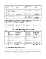
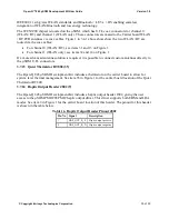
pinout for this header is shown in the table below.
Table 12 - Sensor Expansion Header J2100 Pinout
Pin
No
Signal
Description
Pin
No
Signal
Description
1
SSC0_QUP0_0_I2C1_SDA
CPU Sensor Core
SSC_GPIO0
2
GPIO117_ACCEL_INT
CPU GPIO117
3
SSC1_QUP0_1_I2C1_SCL
CPU Sensor Core
SSC_GPIO1
4
GPIO123
CPU GPIO123
5
GPIO63_QUA_MI2S_DATA
3
CPU GPIO63
6
GPIO118_GYRO_INT
CPU GPIO118


