


Figure 3-7 Clear CMOS Jumper ............................................................................. 3-10
Figure 3-8 BIOS Recovery Jumper .......................................................................... 3-11
Figure 3-9 ME Firmware Recovery Jumper .............................................................. 3-11
Figure 3-10 Intruder Header..................................................................................... 3-11
Figure 3-11 QPI Slow Jumper ................................................................................. 3-12
Figure 3-12 NMI Jumper ......................................................................................... 3-12
Figure 3-13 Force ME Upgrade Jumper .................................................................. 3-13
Appendix Figure I China RoHS Regulations ................................................................. I
List of Tables
Table i Product Safety Requirements ........................................................................... vi
Table ii European Union EMC Requirements ............................................................. viii
Table 1-1 Manual Introduction ..................................................................................... 1-1
Table 1-2 Product Features ....................................................................................... 1-2
Table 1-3 LED Information of NIC Port ...................................................................... 1-7
Table 1-4 LED Information of Management Port ....................................................... 1-7
Table 1-5 ID LED Information .................................................................................... 1-7
Table 3-1 Pin Definition of PCH SSATA / PCH SATA Connector (J1) ......................... 3-1
Table 3-2 Pin Definition of PCH SATA Connector (J42) ............................................. 3-2
Table 3-3 Pin Definition of PCH SATA Connector (J32) ............................................. 3-2
Table 3-4 Pin Definition of PCH SATA Connector (J34) ............................................. 3-3
Table 3-5 Pin Definition of SATA SGPIO Connector (J41) ......................................... 3-3
Table 3-6 Pin Definition of MINI-SAS Connector (J3) ................................................ 3-4
Table
3-7 Pin Definition of MINI-SAS Connector (J24) ............................................. 3-5
Table 3-8 Pin Definition of Middle Plane Connector (J76) ......................................... 3-6
Table 3-9 Pin Definition of Middle Plane Connector (J77) ......................................... 3-8
Table 3-10 Clear Password Jumper Function ............................................................ 3-10
Table 3-11 Clear CMOS Jumper Function ................................................................. 3-10
Table 3-12 BIOS Recovery Jumper Function ........................................................... 3-11
Table 3-13 ME Firmware Recovery Jumper Function ............................................... 3-11
Table 3-14 Intruder Header Function ........................................................................ 3-11
Table 3-15 QPI Slow Jumper Function .................................................................... 3-12
Table 3-16 NMI Jumper Function ............................................................................ 3-12
Table 3-17 Force ME Upgrade Jumper Function ..................................................... 3-13
Summary of Contents for B900G3
Page 1: ...Board Manual B900G3 August 2015 Revision A P N 2015 MNU 000006 ...
Page 3: ......
Page 8: ......
Page 18: ......
Page 28: ......
Page 29: ......
Page 30: ......
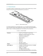
Page 38: ...Hardware Operations 2015 MNU 000006 2 8 Figure 2 13 DIMM Socket Location ...
Page 42: ......
Page 56: ......
Page 57: ...Appendix China RoHS Regulations ...
Page 58: ......
Page 59: ......
Page 60: ......


