background image


41 

2.

 INDEX 

1

2

3

4

5

6

A

B

C

D

6

5

4

3

2

1

D

C

B

A

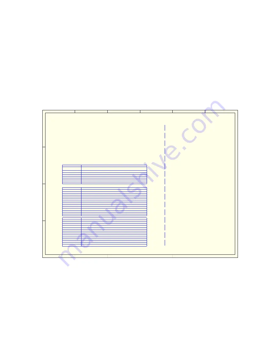
FUNCTION

Reserved for 16Mbit Flash Bank Switch Control

Program storage

System Clock Requirement

EAUXx

FUNCTION

24C02 SERIAL EEPROM

DA1196/DA1131

Background

Not Used.

FUNCTION

Layout----Hermoine GRANGER Revision-A3B2


Base on MTK Reference Design COMMON79_HD60_V2,Re-sized for Complete Loader PCB Dimension Requirement.

Memories Required

System setup configuration storage

Hermoine GRANGER Revision-A3

Revision History

The current MT1379xE requires 8M bit Flash for DVD code storage & slow speed code running. For SDRAM, only 4M byte space is required. This
provides a lower cost option to use 2 pieces 1Mx16 SDRAM with 32bit data width. The other option is to use one single piece of higher density
4Mx16 SDRAM & the extra memory space will be used as track buffer for better anti-shock function.

MT1379xE only requires a single 27MHz clock to operate. This clock can either be generated externally and feed into pin 187 or thru a 27MHz crystal
attached to pin 186 and 187.  This 27Mhz will be used for all video processing reference. In addition, on chip PLL circuits generate all operating
frequency for the integrated MPEG decoder RISC+DSP, Read Channel DSP+Servo circuitry,  8032 core system controller & audio clock.

System Configuration

32/64MBit SDRAM

Sapre

I2C Bus Serial Data Signal

DVD pickup actuators & Traverse motors driver

6-Channel/2-Channel AudioDAC

CHIP

MT1379xE

8032 Core P1.2


This design is the Servo-MPEG Board of COSMIC Technology Co., LTD. DVD Complete Loader module DCL34MK-72/75, which is thecombination of this PCBA & Cosmic DV-34 Pickup Loader.

8Mbit FLASH

MT1379E Pin 157

AUX I/O Port


Super integration chip that handles all Servo, Read Channel, DVD Decoding and system control. Built-in TV-Encoder direct drives a TV set.

Revision-A1

Data storage and frame buffer

Revision-A2

1. Add Audio ADC, DA1196 Software Control Mode Option.

MT1336E

Analog front end CMOS IC for MT13x9E DVD chip.

BA5954FP

BA6208F

Disc loading tray motor driver.


Servo-MPEG Board of MAXITECH Complete Loader DCL34MK72/75MT1379xE for Cosmic DV-34 Pickup Loader

FSG@COSMICTEC.COM

8032 Core P1.3

8032 Core P1.4

8032 Core P1.5

8032 Core P1.6

8032 Core P1.7

8032 Core P3.0

8032 Core P3.1

Front Panel Display Driver Serial Interface Data Signal

I2C Bus Serial Clock & Front Panel Display Driver Serial Interface Clock Signal

Spare

Spare

8032 Core P3.2

8032 Core P3.3

8032 Core P3.4

8032 Core P3.5

8032 Core P3.6

8032 Core Interrupt#0, Chip Intrenal Use.

8032 Core Interrupt#1, Infrared Remote Control Serial Data Receive.

8032 Core RS-232 port RxD Signal.

8032 Core RS-232 port TxD Signal.

8032 Core P3.7

8032 Core Write Enable Signal, Chip Internal Use.

8032 Core Read Enable Signal, Chip Internal Use.

This design is based on MTK second generation MT1379xE super integration DVD chipset. The MT1379xE is built upon MTK's proven previous
MT1369xE super integration chipset. It supported all MT1369xE generation features plus new features including Progressive Scan output with
built-in very high performance 6-channdel 12 bit TV-Encoder (Macrovision compliance) and Dolby ProLogic II surround sound processing. With
the chipset's highest integrity, a complete DVD design can now be implemented with minimum chip count & external components.

MT1379E Pin 158

MT1379E Pin 175

MT1379E Pin 176

MT1379E Pin 177

MT1379E Pin 179

MT1336E IO0:4

Audio Output MUTE Control Signal.

SCART Control Signal FS1.

Video Horizontal Synchronization Signal HSYNC# or SCART Control Signal RGB/Video Switch.

MIC MUTE Control Signal.

Disc Loading Tray In Position Limit Switch Detect.

Not Used

Video Vertical Synchronization Signal VSYNC# or SCART Control Signal FS0.

MT1336E IO5

MT1336E IO6

MT1336E IO7

MT1336E IO8

MT1336E IO9

MT1336E IOA

MT1336E IOB

Disc Loading Tray Out Position Limit Switch Detect.

Pickup Head Home Position Limit Switch Detect.

Motor Driver Stand-by Control.

ENDM

Pickup Head CD/DVD Switch.

PCB Layout GRANGER-A2B1

2. 1Mx16 SDRAM Connection Data DQ[16:31] Changed.

Revision-A3

1. Based on Rev-A2, Video Output Buffer Added.

PCB Layout GRANGER-A3B2

Disc Loading Tray Close Drive Signal.

Front Panel Display Driver Serial Interface Strobe Signal

PCB Layout GRANGER-A4B3

Revision-A4

1. Based on Rev-A3, VFD Interface STB Signal Changed from P1.2 to P1.3.

2. VFD Interface I/O Changed.


3. Fixed Some KnownErrors.


1. Some Ferrite Beads on Power Supply Path Changed fromSMD0805 to SMD1206.


Summary of Contents for DVD-636

Page 1: ...MTK1379SOLUTION MODEL DVD 636 DVD PLAYER...

Page 2: ...d IC MT1336 6 2 1 3 28 Pin 24 Bit 192kHz D A with Volume Control DA1196 15 2 1 4 Serial EEPROM 16K 2048 x 8 24C16 17 2 1 5 8M BIT 1Mx8 512Kx16 CMOS FLASH MEMORY 18 2 1 6 512K X 16 Bit X 2 Banks Synchr...

Page 3: ...current tester or a metering system that complies with American National Standards institute ANSI C101 1 Leakage Current for Appliances and underwriters Laboratories UL 1270 40 7 With the instrument s...

Page 4: ...higher voltage wattage etc Parts that have special safety characteristics are identified by shading an or a on schematics and parts lists Use of a substitute replacement that does not have the same s...

Page 5: ...ing techniques of component damage caused by static electricity 1 immediately before handling any semiconductor components or semiconductor equipped assembly drain off any electrostatic charge on your...

Page 6: ...t Descriptions 2 1 1 DVD SANYO HD60 PUH Connector Pin Definition I F Signals I O Pin F 1 F 2 T 3 T 4 C 5 D 6 CD DVD 7 RF 8 A 9 B 10 F 11 GND PD 12 VC 13 VCC 14 E 15 NC 16 VR CD 17 VR DVD 18 LD CD 19 M...

Page 7: ...rection PLI Focus Tracking Loading AuDdio D A WM8720 SDRAM 1 16MHzX2 Video D A CS4955 1 F Conn frant pannel Spindle Motor Focus Coil Track Coil Sied Motor Loading Motor BA5954FP 4ch motor Drive BA6208...

Page 8: ...n mix audio output for DolbyTM Dolby Pro Logic Linear PCM streams for24 bit 96KHz Concurrent S PDIF out and 2 channel audio output Sensaura Dolby Digital Virtual Surround DTS Digital Surround 2 channe...

Page 9: ...7 Pinout Diagram...

Page 10: ...UP3_5 UWR URD DVSS RD7 RD6 RD5 RD4 DVDD2 RD3 RD2 RD1 RD0 RWE CAS RAS RCS BA0 DVSS RD15 RD14 RD13 RD12 DVDD3 RD11 RD10 RD9 RD8 DVSS CLK CLE RFIP RFIN RFDTSLVN FEI CSO RFDTSLVP TEZISLV RFSUBI ADIN ADCV...

Page 11: ...t pull up Motor Hall sensor input 21 DVSS Ground Ground 22 HIGHA0 Inout pull up Microcontroller address 8 23 HIGHA1 Inout pull up Microcontroller address 9 24 HIGHA2 Inout pull up Microcontroller addr...

Page 12: ...active low 77 DVSS Ground Ground 78 RD7 Inout DRAM data 7 79 RD6 Inout DRAM data 6 80 RD5 Inout DRAM data 5 81 RD4 Inout DRAM data 4 82 DVDD2 Power 2 5V power 83 RD3 Inout DRAM data 3 84 RD2 Inout DRA...

Page 13: ...D20 Inout pull up down DRAM data 20 143 RD19 Inout pull up down DRAM data 19 144 RD18 Inout pull up down DRAM data 18 145 DVSS Ground Ground 146 RD17 Inout pull up down DRAM data 17 147 RD16 Inout pul...

Page 14: ...egative input of RF differential signal 216 RFIP Analog input Positive input of RF differential signal MT1336 GENERAL DESCRIPTION MT1336 is a high performance CMOS analog front end IC for both CD_ROM...

Page 15: ...RF Ripple P 18 4 WOBBLE Detection P 19 Command Access Timings P 20 Programmable I O P 21 Register 1 Register Map P 22 24 2 Register Description P 25 50 MT1336 PIN DESCRIPTIONS Pin Numbers Symbol Type...

Page 16: ...apacitor 122 AGC3 Analog Wobble AGC loop3 capacitor 127 RFSUBO Analog output Header push pull RF output signal 1 WOBSO Analog output Wobble signal output 6 RFOP Analog output RF positive output 7 RFON...

Page 17: ...plifier for hall sensor signal 75 REFSIN Analog input Positive input of amplifier for hall sensor signal 76 SINPHI Analog output Amplifier output for hall sensor signal 71 HALLCOS Analog input Negativ...

Page 18: ...16 Features APPLICATIONS CD DVD audio Home theare systems Set top boxes PIN DESCRIPTIONS Note Digital input pins have Schmitt trigger input buffers...

Page 19: ...K or 2048 x 8 16K 2 Wire Serial Interface Schmitt Trigger Filtered Inputs for Noise Suppression Bi directional Data Transfer Protocol 100 kHz 1 8v 2 5V 2 7V and 400 kHz 5V Compatibility Write Protect...

Page 20: ...m active current 0 2uA typical standby current Command register architecture Byte word Programming 7us 12us typical Sector Erase Sector structure 16K Bytex1 8K Bytex2 32K Bytex1 and 64K Byte x15 Auto...

Page 21: ...lows code changes in previously locked sectors 100 000 minimum erase program cycles Latch up protected to 100mA from 1V to VCC 1V Boot Code Sector Architecture T Top Boot Sector B Bottom Boot Sector L...

Page 22: ...X 2 Banks Synchronous DRAM A43L0616 Features JEDEC standard 3 3V power supply LVTTL compatible with multiplexed address Dual banks Pulse RAS MRS cycle with address key programs CAS Latency 2 3 Burst L...

Page 23: ...tial interleave All inputs are sampled at the positive going edge of the system clock Burst Read Single bit Write operation DQM for masking Auto self refresh 64ms refresh period 4K cycle 50 Pin TSOP I...

Page 24: ...s Row address RA0 RA10 Column address CA0 CA7 BA Bank Select Address Selects bank to be activated during row address latch time Selects band for read write during column address latch time RAS Row add...

Page 25: ...rformance Video Out 1 Vpp into 75 ohm S Video Out Y 1Vpp into 75 ohm C 0 286 Vpp into 75 ohm D A Converter 27MHz 10bit Audio Performance Frequency Response DVD fs 48 96KHz 4Hz 22 44KHz Video CD fs 44...

Page 26: ...e 4 Do not shut down the player during upgrade it will restart automatically after upgrade 5 Upgrade finish How to change the region code 1 Power on the machine and press OPEN button to push the tray...

Page 27: ...25 5 Operating Instruction Please refer to the User s Manual for operation instruction of the system...

Page 28: ...dle clean and protect discs Do not touch the playing side of a disc Do not stick any paper or glue strip on a disc How to clean discs Finger prints and dust on surface can affect the sound and picture...

Page 29: ...compatible disc Check the disc format and its colour system The disc is placed upside down Load a compatible disc Check the disc format and its colour system The disc not put in the tray correctly Che...

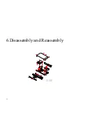
Page 30: ...28 6 Disassembly and Reassembly...

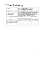
Page 31: ...formed with the remote controller Check the batteries are installed with the correct polarities Point the remote control unit at the remote control sensor and operate Remove the obstacles between the...

Page 32: ...ader to MPEG board 5PIN 2 54mm L 500mm 1 MPEG board 4PIN 2 54mm L 120mm 1 control panel to power board 6PIN 2 54mm L 450mm 1 control panel to MPEG board 13PIN 2 0mm L 100mm 1 output board to MPEG boar...

Page 33: ...iper22 CO DCC602 control panel CO DCCC602 control panel 1 AV output board CO DOB1379 1 with SCART Optical and KARAOKE without earphone 4 plastical sets DVD 636 front panel CO 602 front panel 1 power s...

Page 34: ...O 602HBA 1 black bolt 3 8BAUU 12 9 for control panel 2 for power botton 1 for bracket bolt 3 8BAUU 8 8 for Audio output jack bolt 3 15BBHE 8 5 for power board 3 for AV output board bolt 3 6WBHE 11 4 f...

Page 35: ...0 260mm 1 for owner s manual bag 480 580mm 1 pearl cotton B appendix DVD 636 remote control 1 remote control batteries 7 1 set DVD 636 manual 1 Video connection wire 1 5M 1 Audio connection wire 1 5M...

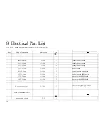
Page 36: ...0 5mm 1 C15 Ceramic capacitor 100pF 63V 20 Y5P 5mm 3 C11 C12 C13 Ceramic capacitor 10nF 1KV _ 10 5mm 1 C8 Electrolytic capacitor 220UF 16V 20 6X11mm 1 C10 none HL D116 VFD Electrolytic capacitor 470UF...

Page 37: ...7 4 D1 D2 D3 D4 Diode IN5404 2 D13 D14 Diode SR560 1 D10 Schottky Diode HER107 5 D6 D7 D8 D9 D12 Schottky Diode UF4007 1 D5 Zener Diode 3 3V 1 2W 1 DZ1 Fuse T2A T D 250V PL UL CSA VDE 1 F1 Fuse Jack B...

Page 38: ...n Film Resistor 1 4W 75K 5 1 R8 Press sensitive Resistor 07 471 1 RV1 Grounding solder slice D3 2 mm 3 1 2 3 IC TEA1523P 1 U1 IC TL431 TO 92 decal 1 U3 Photo electric Couple PC817 1 U2 Power Board PCB...

Page 39: ...6 6 5 10 NEXT STOP PREV OPEN REV FWD PAUSE PLAY STOP1 PLAY1 Potentiometer RV0902N 15FD1 A20K P 2 VOL1 VOL2 Jumper 6mm 4 JMP1 JMP3 JMP6 JMP17 Jumper 7mm 2 JMP7 JMP8 Jumper 8mm 3 JMP2 JMP15 JMP16 Jumper...

Page 40: ...38...

Page 41: ...39 10 Circuit Diagrams 1 Control Part 2 INDEX 3 SERVO RF 4 Servo DSP MPEG Memories 5 Audio Video D A 6 AV PORT 7 Power Part...

Page 42: ...K9 KS3 KS4 KS5 K1 K2 LED1 GR6 6 GR7 7 SG1 8 SG2 9 SG3 10 SG4 11 SG5 12 SG6 13 SG7 14 SG8 15 GR3 3 LED GR5 5 GR4 4 GR2 2 GR1 1 IC1 LED 15PIN SG7 KS7 14 SEG6 KS6 13 SEG5 KS5 12 SEG4 KS4 11 SEG3 KS3 10...

Page 43: ...FSG COSMICTEC COM 8032 Core P1 3 8032 Core P1 4 8032 Core P1 5 8032 Core P1 6 8032 Core P1 7 8032 Core P3 0 8032 Core P3 1 Front Panel Display Driver Serial Interface Data Signal I2C Bus Serial Clock...

Page 44: ...9 WGAND 118 SGND 117 TNI 116 TPI 115 SVDD 114 CDFON 113 CDFOP 112 SD 111 SC 110 AVDD 109 IR 108 AGND 107 SB 106 SA 105 MD 104 MC 103 VFO13 38 VDD 37 AGNDX 36 AGNDX 35 AGNDX 34 DPFO 33 DPFN 32 GNDP 31...

Page 45: ...RD21 141 DVDD2 140 RD22 139 RD23 138 DQM2 137 DQM3 136 DVSS 135 RD24 134 RD25 133 RD26 132 RD27 131 DVDD3 130 RD28 129 RD29 128 RD30 127 RD31 126 DVSS 125 RA3 124 RA2 123 RA1 122 RA0 121 DVDD2 120 RA...

Page 46: ...56 0 1u 1 2 3 4 5 6 7 8 9 10 11 12 13 CN6 Video Output JST13 Pin 2 0mm Pitch C53 100u C54 10u R2 RES R3 RES R85 160 1 Q8 3906 R81 RES CB106 0 1u R80 75Ohm 0805 CB23 0 1u R59 RES CB12 0 1u R108 160 1 Q...

Page 47: ...1 10P L3 1 8UH DIP VGND VGND VGND T SY SY C400 220P C402 100P C403 22P C401 10P L4 1 8UH DIP VGND VGND VGND T SC SC C500 220P C502 100P C503 22P C501 10P L5 1 8UH DIP VGND VGND VGND T R V R V C600 220...

Page 48: ...265V BC6 102 400V 1 2 3 4 5 CN1 VCC 1 GND 2 RC 3 REG 4 AUX 5 Source 6 NC 7 Drain 8 U1 SST_Viper22 L2 BEAD D5 HER108 C8 103 1KV R7 100K 2W U3 TL431 R5 1 2 3 C3 104 POW SW1 R11 3K 21V 8 6 2 4 10 11 17 1...

Page 49: ...VGND MUTE 27V AGND DQ18 GND AGND ASPDIF 3V3 GND 5V CVBS MO SC B LEF GND FS1 3V3 MO DQ16 R CLK VGND MO GND 5V TUN_L B MIC MUTE GND GND R AGND CENT GND VCC VGND HSW 12V DQ18 SY AGND SL STB GND AGND 5V...

Reviews: