iSYSTEM, October 2016
36/69
14-pin 2.54mm MPC5xxx Cable Adapter
Ordering code
IC50150
This adapter is used to connect the iC5000 / iC5500 / iC6000 development system to Freescale MPC5xxx and
ST SPC56 based target via JTAG debug interface. It connects to Debug/Trace module on one side and to the
target debug connector on the other side. It can be used for targets featuring 14-pin 2.54mm pitch target debug
connector with MPC5xxx pinout.
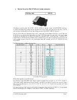
The following pinout is valid on the target side:
Signal
direction
Signal description
Signal
Pin Pin Signal
Signal description
Signal
direction
O
Standard JTAG
TDI
1
2
GND
Ground
I
Standard JTAG
TDO
3
4
GND
Ground
O
Standard JTAG
TCK
5
6
GND
Ground
O
EVTIN
7
8 PORST*
Power On Reset*
O
I/O
System Reset
nSRST
9
10
TMS
Standard JTAG
O
I
Reference voltage
VTref
11 12
GND
Ground
Not connected
NC
13 14 JCOMP (optional) Standard JTAG
O
14-pin MPC5xxx & SPC56 target pinout
Mandatory pins on the microcontroller side are GND, VDD, RESET, TMS, TDI, TDO and TCK.
*Note: Pin 8 (Power on reset) is supported with adapter revision C1 or newer.
JCOMP is an optional pin. Some microcontrollers don’t have this pin. Internally, this is actually JTAG TRST
which resets JTAG TAP state machine. Because JTAG TAP state machine can be reset also by TMS and TCK,
this pin is optional also for the debugger. If microcontroller has JCOMP pin but it is not connected to the target
debug connector then it must be set to non-active state in the target via a pull-up resistor. If not then JTAG TAP
state machine remains in reset and debugging is not possible.
14-pin 2.54mm MPC5xxx Cable Adapter features resettable fuses on all connected pins. These protect debug
signals against overcurrent and cycle back to a conductive state after the excessive current fades away.
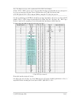
Jumper J1 (TCK)
Note: Jumper J1 was introduced with rv: D1, previous versions (rv: A1, A2, B1, C1, C2) do not have this
jumper.
If the TCK (debug JTAG clock) signal path from the target debug connector to the target microcontroller is not
designed as single point to point connection, user may experience signal integrity problems. For example, the
TCK electrical signal degrades if it’s is routed to multiple points, e.g. to the target microcontroller and also to
some other IC(s), or expansion connector(s) or even to another PCB. In such cases, signal integrity gets
improved by adding a buffer on the TCK driver side (J1: position 2-3).
Normally jumper J1 should be kept in default 1-2 position. When experiencing problems with the initial debug
connection or later unstable operation of the debugger, position 2-3 should be tested too.


