background image


REL 1.2 

Page 41 of 82 

i.MX6 Qseven PMIC SOM Hardware User Guide


iWave Systems Technologies Pvt. Ltd. 

Pin 

No. 

Qseven Edge 

Connector 

Pin Name 

Signal Name 

i.MX6 Ball 

Name/  

Pin Number 

Signal Type/ 
Termination 

Description 

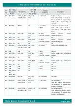
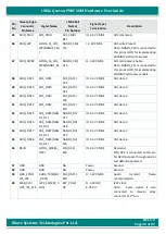
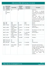
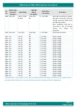
209 

MFG_NC1 

UART2_TXD(EI
M_D26) 

JTAG_TDO/ 
G6 

O, 3.3V CMOS 

Serial data transmitter for debug. 
EIM_D26 is connected to this pin 
through resistor (for UART2_TXD) 
and default populated. 

Note:  Optionally  JTAG_TDO  is 
connected  to  this  pin  through 
resistor 

and 

default 

not 

populated.


210 

MFG_NC3 

JTAG_TMS 

JTAG_TMS/ 
C3 

I, 3.3V CMOS 

JTAG Test Mode Select. 

211 

VCC 

VCC_5V 

NA 

I, 5V Power 

Supply Voltage. 

212 

VCC 

VCC_5V 

NA 

I, 5V Power 

Supply Voltage. 

213 

VCC 

VCC_5V 

NA 

I, 5V Power 

Supply Voltage. 

214 

VCC 

VCC_5V 

NA 

I, 5V Power 

Supply Voltage. 

215 

VCC 

VCC_5V 

NA 

I, 5V Power 

Supply Voltage. 

216 

VCC 

VCC_5V 

NA 

I, 5V Power 

Supply Voltage. 

217 

VCC 

VCC_5V 

NA 

I, 5V Power 

Supply Voltage. 

218 

VCC 

VCC_5V 

NA 

I, 5V Power 

Supply Voltage. 

219 

VCC 

VCC_5V 

NA 

I, 5V Power 

Supply Voltage. 

220 

VCC 

VCC_5V 

NA 

I, 5V Power 

Supply Voltage. 

221 

VCC 

VCC_5V 

NA 

I, 5V Power 

Supply Voltage. 

222 

VCC 

VCC_5V 

NA 

I, 5V Power 

Supply Voltage. 

223 

VCC 

VCC_5V 

NA 

I, 5V Power 

Supply Voltage. 

224 

VCC 

VCC_5V 

NA 

I, 5V Power 

Supply Voltage. 

225 

VCC 

VCC_5V 

NA 

I, 5V Power 

Supply Voltage. 

226 

VCC 

VCC_5V 

NA 

I, 5V Power 

Supply Voltage. 

227 

VCC 

VCC_5V 

NA 

I, 5V Power 

Supply Voltage. 

228 

VCC 

VCC_5V 

NA 

I, 5V Power 

Supply Voltage. 

229 

VCC 

VCC_5V 

NA 

I, 5V Power 

Supply Voltage. 

230 

VCC 

VCC_5V 

NA 

I, 5V Power 

Supply Voltage. 

¹ Important Note: These signals are also used for i.MX6 CPU bootstrap setting on SOM and so no external loads or 

pull-up/pull-down resistors to be connected to these pins which will change the boot configuration. 

Summary of Contents for i.MX6 Qseven PMIC SOM

Page 1: ...REL 1 2 Page 1 of 82 i MX6 Qseven PMIC SOM Hardware User Guide iWave Systems Technologies Pvt Ltd iW RainboW G15M i MX6 Qseven PMIC SOM Hardware User Guide ...

Page 2: ...ed Table 11 Debug UART Header pinout detail is corrected Important Note is added below Table 16 for power sequencing related i MX6 QuadPlus and DualPlus CPU supported Qseven SOM part numbers are updated in ORDERING INFORMATION 2GB RAM supported Qseven SOM part numbers are updated in ORDERING INFORMATION PROPRIETARY NOTICE This document contains proprietary material for the sole use of the intended...

Page 3: ... errata and associated issues Trademarks All registered trademarks product names mentioned in this publication are the property of their respective owners and used for identification purposes only Certification iWave Systems Technologies Pvt Ltd is an ISO 9001 2008 Certified Company Warranty RMA Warranty support for Hardware 1 Year from iWave or iWave s EMS partner For warranty terms go through th...

Page 4: ...1 DDR3 SDRAM 18 2 6 2 SPI NOR Flash 18 2 6 3 eMMC Flash 18 2 6 4 Micro SD Slot 18 2 7 Qseven PCB Edge Connector 19 2 7 1 PCIe Interface 20 2 7 2 Data UART Interface UART5 20 2 7 3 Gigabit Ethernet Interface 20 2 7 4 SATA Interface 21 2 7 5 USB 2 0 Host Interface 21 2 7 6 USB 2 0 OTG Interface 22 2 7 7 SD MMC Interface 22 2 7 8 AC 97 I2S Audio Interface 22 2 7 9 LVDS Display Interface 23 2 7 10 HDM...

Page 5: ... 10 1 NAND Flash 60 2 10 2 RTC Controller 60 2 10 3 PMIC OTP Header 61 2 10 4 JTAG Header 62 2 10 5 Debug UART Header 64 2 10 6 Power IN Connector 65 3 TECHNICAL SPECIFICATION 66 3 1 Electrical Characteristics 66 3 1 1 Power Input Requirement 66 3 1 2 Power Input Sequencing 67 3 1 3 Power Consumption 68 3 2 Environmental Characteristics 69 3 2 1 Environmental Specification 69 3 2 2 Heat Spreader 6...

Page 6: ...tion procedure 73 Figure 18 Silk Screen Top View 80 Figure 19 Silk Screen Bottom View 81 Figure 20 i MX6 Qseven PMIC SOM Development Platform 82 List of Tables Table 1 Acronyms Abbreviations 7 Table 2 Terminology 9 Table 3 Boot Mode Settings Truth Table 16 Table 4 Compatible Magnetics 21 Table 5 230 Pin PCB Edge Connector Pin Assignment 27 Table 6 Expansion Connector1 Pin Assignment 45 Table 7 Exp...

Page 7: ...ave specified pin outs based on the high speed MXM system connector that has a standardized pin out regardless of the vendor A single ruggedized MXM connector provides the carrier board interface to carry all the I O signals to and from the Qseven module 1 3 List of Acronyms The following acronyms will be used throughout this document Table 1 Acronyms Abbreviations Acronyms Abbreviations ARM Advan...

Page 8: ...a Local Bus MMC Multi Media Card NC No Connect NPTH Non Plated Through hole PCB Printed Circuit Board PMIC Power Management Integrated Circuit PTH Plated Through hole PWM Pulse Width Modulation RGMII Reduced Gigabit Media Independent Interface ROM Read Only Memory RTC Real Time Clock SATA Serial Advanced Technology Attachment SD Secure Digital SDIO Secure Digital Input Output SDRAM Synchronous Dyn...

Page 9: ...MDS Transition Minimized Differential Signal DIFF Differential Signal OD Open Drain Signal OC Open Collector Signal RS232 RS 232 compatible Signal Power Power Pin PU Pull Up PD Pull Down NA Not Applicable NC Not Connected Important Note Signal Type does not include internal pull ups or pull downs implemented by the chip vendors and only includes the pull ups or pull downs implemented On SOM 1 5 Re...

Page 10: ...If CPU pin functionality name and pad name is different Signal name is mentioned as Functionality name CPU Pad name Example UART3_RTS SD3_RST In this signal UART3_RTS is the functionality which we are using and SD3_RST is the CPU Pad name If CPU pin functionality is GPIO Signal name is mentioned as GPIO Number_FunctionalityDescription CPU Pad name Example GPIO7_0_SD1_CD SD3_DAT5 In this signal GPI...

Page 11: ...ST1 HS PHY LVDS0 LVDS1 PWM HDMI 1 4 10 100 1000 ENET eSDHC1 eCSPI2 CAN1 UART5 WDOG1 GPIOs MMC 8bit SPI DDR3 64bit Micro SD Connector SD 4bit Expansion Connector1 80Pin header USB 2 0 Hub 4Port Gigabit Ethernet PHY MMDC eCSPI1 eSDHC4 eSDHC3 Audio x 1 AUDMUX4 UART2 LCD 24bpp x 1 MIPI DSI x 1 DISP0 MIPI DSI UART1 UART3 ESAI SPDIF CSI1 KPP UART with CTS RTS x 2 ESAI x 1 SPDIF x 1 Camera2 8bit x 1 Keyp...

Page 12: ...itch Boot Media Setting Switch Memory 1GB DDR3 RAM Expandable 2MB SPI NOR Flash Expandable 4GB eMMC Flash Expandable Micro SD slot Network Communication Gigabit Ethernet PHY transceiver USB 2 0 High Speed 4 Port Hub Qseven PCB Edge Interfaces PCIe Gen2 0 x 1 Port Data UART x 1 Port Gigabit Ethernet x 1 Port through On SOM Gigabit Ethernet PHY transceiver SATA II 3 0 Gbps x 1 Port USB Host 2 0 x 4 ...

Page 13: ...lel Camera1 8bit x 1 Port ESAI x 1 Port SPDIF x 1 Port Data UART with CTS RTS x 2 Ports Expansion Connector2 Interfaces Parallel Camera2 8bit x 1 Port Four Lane MIPI CSI Memory Bus Address Data Multiplexed x 1 Port Keypad Interface 3x3 Data UART x 1 Port MLB x 1 Port Optional Features NAND Flash RTC Controller PMIC OTP Header JTAG Header Debug UART Header for Standalone usage Power IN Connector fo...

Page 14: ...nt in integrated multimedia application processors which is part of growing multimedia focused products that offers high performance processing and are optimized for lowest power consumption The Block Diagram of i MX6Q D CPU from the Freescale s i MX6Q D datasheet is shown below for your reference Figure 2 i MX6Q Simplified Block Diagram Note Please refer the latest i MX6 Datasheet Reference Manua...

Page 15: ...nce and timing i MX6 CPU s I2C2 interface is used for PMIC programmable I2C address for PMIC is 0x08 2 5 Boot Switches i MX6 CPU boot process begins at Power On Reset POR where the hardware reset logic forces the ARM core to begin execution starting from the on chip boot ROM i MX6 CPU Boot ROM code uses the state of the internal register BOOT_MODE 1 0 as well as the state of various eFUSEs and or ...

Page 16: ...Table 3 Boot Mode Settings Truth Table Boot Mode Setting On i MX6 Qseven PMIC SOM Description SW2 2 Position Switch POS1 POS2 Image Internal Boot Mode Default In this mode i MX6 boot media is selected by GPIO Pin s settings OFF ON Boot From eFuses In this mode i MX6 boot media is selected by i MX6 eFUSE settings Note i MX6 eFuse setting is not modified by iWave from silicon shipped value OFF OFF S...

Page 17: ...supports different boot media options for booting i MX6 CPU as mentioned in the below table Boot Media Setting On i MX6 Qseven PMIC SOM SW1 8 Position Switch POS1 POS2 POS3 POS4 POS5 POS6 POS7 POS8 Image eCSPI1 SPI Flash Default ON ON OFF X X X X X SD4 8bit eMMC OFF ON ON ON ON OFF ON OFF SD3 4bit Micro SD OFF OFF ON OFF ON ON OFF OFF SD1 4bit Through Qseven Edge OFF OFF ON OFF OFF ON OFF OFF SD1 ...

Page 18: ...controller of the i MX6 CPU and operates at 3 3 Voltage level The SPI flash memory is physically located on bottom side of the Qseven SOM 2 6 3 eMMC Flash i MX6 Qseven PMIC SOM supports 4GB eMMC expandable memory as mass storage and also can be used as boot device eMMC is directly connected to the uSDHC4 of the i MX6 CPU and operating at 3 3 Voltage level The eMMC flash memory is physically locate...

Page 19: ...Qseven Specification 2 0 The interfaces which are available at 230pin Qseven Edge connector are explained in the following sections Figure 5 Qseven PCB Edge Connector Number of Pins 230 Connector Part Not Applicable On Board PCB Edge connector Mating Connector IMSA 18010S 230A GN1 from IRISO AS0B326 S78N 7F from FOXCONN 88882 2D0K from Aces CN113 230 0001VE from Yamaichi Electronics ...

Page 20: ...n connector1 and one more on Expansion connector2 i MX6 CPU s UART5 controller is used for Data UART interface on Qseven Edge connector which supports Serial RS 232NRZ mode 9 bit RS 485 mode and IrDA mode It is compatible with High speed TIA EIA 232 F up to 5 0 Mbit s with auto baud rate detection up to 115 2 Kbit s It supports 7 or 8 data bits for RS 232 characters 9 bit RS 485 format 1 or 2 stop...

Page 21: ...for SATA Interface which can support SATA II with transfer rate of 3Gbps and backward compatible to SATA I with transfer rate of 1 5Gbps i MX6 CPU s SATA PHY output is connected to Qseven Edge connector SATA channel 0 Also SATA activity LED output is supported on Qseven edge connector from i MX6 CPU GPIO GPIO4_10 For more details refer Qseven Edge connector pins 29 31 33 35 37 on Table 5 Note SATA...

Page 22: ...10 It supports 1 bit or 4 bit transfer mode for SD and SDIO cards up to UHS I SDR104 mode 104 MB s max Also i MX6 CPU s USDHC1 is fully compliant with Multimedia Card System Specification v4 2 4 3 4 4 4 41 including high capacity cards size 2GB It supports 1 bit 4 bit or 8 bit transfer mode for MMC cards up to 52 MHz in both SDR and DDR modes 104 MB s max i MX6 Qseven PMIC SOM supports SDIO card d...

Page 23: ...tness control output is supported on Qseven Edge connector from i MX6 CPU s PWM output PWM2 For more details refer Qseven Edge connector pins 99 to 123 on Table 5 Note i MX6 Duallite and i MX6 Solo CPU supports only one IPU and so at any time only two display interfaces including Parallel RGB HDMI MIPI DSI can be supported 2 7 10 HDMI Interface i MX6 Qseven PMIC SOM supports one HDMI display port ...

Page 24: ...en configured as an input it is possible to detect the state of the input by reading the state of an internal register In addition the GPIO peripheral can produce CORE interrupts For more details refer Qseven Edge connector pins 185 to 192 on Table 5 Note Most of the i MX6 Pins which are connected to Qseven Edge connector and Expansion connectors can be configured as GPIO with interrupt capable if...

Page 25: ... MX6 CPU s ONOFF pin This pin can be used to On Off the i MX6 CPU by connecting push button in the carrier board When the board power is On a button press between 750ms to 5s will send an interrupt to core to request software to bring down the i MX6 safely if software supports Otherwise button press greater than 5s results in a direct hardware power down which is applicable when software is unable...

Page 26: ...h is compatible with the standard NXP I2C bus protocol It supports standard mode with data transfer rates up to 100kbps and Fast mode with data transfer rates up to 400kbps i MX6 CPU s I2C1 is connected to General Purpose I2C bus0 of Qseven Edge connector Since flexible I2C standard allows multiple devices to be connected to the single bus i MX6 CPU s I2C1 is also connected to LVDS Display ID DDC ...

Page 27: ...t link status LED Note Same signal is also connected to Qseven edge connector 8th 13th pins So use only in one place 8 GBE_LINK10 00 GPHY_LINK_LED 2 NA O 3 3V CMOS Gigabit Ethernet link status LED Note Same signal is also connected to Qseven edge connector 7th 13th pins So use only in one place 9 GBE_MDI1 GPHY_BTXRXM NA IO DIFF Gigabit Ethernet MDI differential pair 1 negative 10 GBE_MDI0 GPHY_ATX...

Page 28: ...r implementing system wake event if required 18 SUS_S3 NA NA O 3 3V CMOS 10K PU S3 state is not supported Note This pin is pulled up with 10K directly 19 SUS_STAT GPIO6_9_SUS_S TAT NANDF_WP _B NANDF_WP_B E15 O 3 3V CMOS Suspend status Note NANDF_WP_B is connected to this pin as GPIO for implementing suspend status if required 20 PWRBTN CPU_ON_OFF ONOFF D12 I 3V CMOS Power button input Note For mor...

Page 29: ...d SATA0 transmit output differential negative 32 SATA1_TX NC NA NC 33 SATA_ACT GPIO4_10_SATA _ACT KEY_COL2 KEY_COL2 W6 O 3 3V OC SATA command activity line 34 GND GND NA Power Ground 35 SATA0_RX SATA_RXP SATA_RXP B14 I DIFF 0 01uF AC coupled SATA0 receive input differential positive 36 SATA1_RX NC NA NC 37 SATA0_RX SATA_RXM SATA_RXM A14 I DIFF 0 01uF AC coupled SATA0 receive input differential neg...

Page 30: ...D1_DAT0 SD1_DAT0 A21 IO 3 3V CMOS SD1 data 0 50 SDIO_DAT3 SD1_DAT3 SD1_DAT3 F18 IO 3 3V CMOS SD1 data 3 51 SDIO_DAT2 SD1_DAT2 SD1_DAT2 E19 IO 3 3V CMOS SD1 data 2 52 SDIO_DAT5 SD1_DAT5 NAN DF_D1 NANDF_D1 C17 IO 3 3V CMOS SD1 data 5 53 SDIO_DAT4 SD1_DAT4 NAN DF_D0 NANDF_D0 A18 IO 3 3V CMOS SD1 data 4 54 SDIO_DAT7 SD1_DAT7 NAN DF_D3 NANDF_D3 D17 IO 3 3V CMOS SD1 data 7 55 SDIO_DAT6 SD1_DAT6 NAN DF_D...

Page 31: ...to this pin as GPIO for implementing SMB alert functionality if required 65 HDA_SDI I2S_SDI AUD4_TXD SD2 _DAT2 SD2_DAT2 A23 I 3 3V CMOS Audio receive data Note Make sure to enable AUDMUX_PDCR4 register s 12th bit TXRXEN in i MX6 to make this pin as receive 66 GP0_I2C_CLK I2C1_SCL EIM_D 21 EIM_D21 H20 O 3 3V OD 4 7K PU I2C1 clock Note Same signal is also connected to Qseven edge connector 127th 128...

Page 32: ...SB_SSTX0 NC NA NC 78 USB_P6 USB_SSRX0 NC NA NC 79 USB_6_7_OC NC NA NC 80 USB_4_5_OC USB_4_5_OC NA I 3 3V CMOS 10K PU Over current sense for USB port 4 5 81 USB_P5 USB_SSTX1 NC NA NC 82 USB_P4 USB_SSRX1 USB_HUBP4_D M NA IO DIFF USB Host port 4 data negative 83 USB_P5 USB_SSTX1 NC NA NC 84 USB_P4 USB_SSRX1 USB_HUBP4_DP NA IO DIFF USB Host port 4 data positive 85 USB_2_3_OC USB_2_3_OC NA I 3 3V CMOS ...

Page 33: ...S secondary channel differential pair 0 positive 101 eDP0_TX0 LVDS_A0 LVDS0_TX0_N LVDS0_TX0_N U2 O 2 5V LVDS LVDS primary channel differential pair 0 negative 102 eDP1_TX0 LVDS_B0 LVDS1_TX0_N LVDS1_TX0_N Y1 O 2 5V LVDS LVDS secondary channel differential pair 0 negative 103 eDP0_TX1 LVDS_A1 LVDS0_TX1_P LVDS0_TX1_P U3 O 2 5V LVDS LVDS primary channel differential pair 1 positive 104 eDP1_TX1 LVDS_B...

Page 34: ... eDP0_TX3 LVDS_A3 LVDS0_TX3_N LVDS0_TX3_N W2 O 2 5V LVDS LVDS primary channel differential pair 3 negative 116 eDP1_TX3 LVDS_B3 LVDS1_TX3_N LVDS1_TX3_N AA3 O 2 5V LVDS LVDS secondary channel differential pair 3 negative 117 GND GND NA Power Ground 118 GND GND NA Power Ground 119 eDP0_AUX LVDS_A_CLK LVDS0_CLK_P LVDS0_CLK_P V3 O 2 5V LVDS LVDS primary channel differential clock positive 120 eDP1_AUX...

Page 35: ...lso connected to Qseven edge connector 68th 125th pins 127 GP2_I2C_CLK LVDS_DID_ CLK I2C1_SCL EIM_D 21 EIM_D21 H20 O 3 3V OD 4 7K PU I2C1 clock Note Same signal is also connected to Qseven edge connector 66th 128th pins 128 eDP1_HPD LVDS_BLC_ CLK I2C1_SCL EIM_D 21 EIM_D21 H20 O 3 3V OD 4 7K PU I2C1 clock Note Same signal is also connected to Qseven edge connector 66th 127th pins 129 CAN0_TX CAN1_T...

Page 36: ...Power Ground 149 DP_LANE0 TMDS_LANE 2 HDMI_D2P HDMI_D2P K4 O TMDS HDMI differential data lane 2 positive 150 HDMI_CTRL_ DAT I2C2_SDA KEY_ ROW3 KEY_ROW3 T7 IO 3 3V CMOS I2C2 data Note Same signal is also connected to Qseven edge connector 62nd pin 151 DP_LANE0 TMDS_LANE 2 HDMI_D2M HDMI_D2M K3 O TMDS HDMI differential data lane 2 negative 152 HDMI_CTRL_ CLK I2C2_SCL KEY_C OL3 KEY_COL3 U5 O 3 3V CMOS...

Page 37: ...r implementing PCIe reset 159 GND GND NA Power Ground 160 GND GND NA Power Ground 161 PCIE3_TX NC NA NC 162 PCIE3_RX NC NA NC 163 PCIE3_TX NC NA NC 164 PCIE3_RX NC NA NC 165 GND GND NA Power Ground 166 GND GND NA Power Ground 167 PCIE2_TX NC NA NC 168 PCIE2_RX NC NA NC 169 PCIE2_TX NC NA NC 170 PCIE2_RX NC NA NC 171 UART0_TX UART5_TXD KEY _COL1 KEY_COL1 U7 O 3 3V CMOS UART5 serial data transmitter...

Page 38: ...e_RXP B2 O DIFF PCIe differential receive line positive 181 PCIE0_TX PCIe_TXM PCIe_TXM A3 I DIFF 0 1uf AC coupled PCIe differential transmit line negative 182 PCIE0_RX PCIe_RXM PCIe_RXM B1 I DIFF PCIe differential receive line negative 183 GND GND NA Power Ground 184 GND GND NA Power Ground 185 LPC_AD0 GPIO0 GPIO1_8_Q7_G PIO0 GPIO_8 GPIO_8 R5 IO 3 3V CMOS General purpose input output 0 Note Same s...

Page 39: ...lso connected to Expansion connector1 09th pin 191 SERIRQ GPIO6 GPIO1_29_Q7_ GPIO6 ENET_TX D1 ENET_TX_D1 W20 IO 3 3V CMOS General purpose input output 6 Note Same signal is also connected to Expansion connector1 07th pin 192 LPC_LDRQ GPIO7 GPIO1_30_Q7_ GPIO7 ENET_TX D0 ENET_TX_D0 U20 IO 3 3V CMOS General purpose input output 7 Note Same signal is also connected to Expansion connector1 05th pin 193...

Page 40: ... Master serial output Slave serial input 200 SPI_CS0 eCSPI2_SS0 CSI0 _DAT11 CSI0_DAT11 M3 O 3 3V CMOS SPI2 chip select 0 201 SPI_MISO eCSPI2_MISO C SI0_DAT10 CSI0_DAT10 M1 I 3 3V CMOS SPI2 Master serial input Slave serial output 202 SPI_CS1 eCSPI2_SS1 EIM _LBA EIM_LBA K22 O 3 3V CMOS 14 7K PD SPI2 chip select 1 203 SPI_SCK eCSPI2_SCLK CSI 0_DAT8 CSI0_DAT8 N6 O 3 3V CMOS SPI2 clock 204 MFG_NC4 JTAG...

Page 41: ...ltage 215 VCC VCC_5V NA I 5V Power Supply Voltage 216 VCC VCC_5V NA I 5V Power Supply Voltage 217 VCC VCC_5V NA I 5V Power Supply Voltage 218 VCC VCC_5V NA I 5V Power Supply Voltage 219 VCC VCC_5V NA I 5V Power Supply Voltage 220 VCC VCC_5V NA I 5V Power Supply Voltage 221 VCC VCC_5V NA I 5V Power Supply Voltage 222 VCC VCC_5V NA I 5V Power Supply Voltage 223 VCC VCC_5V NA I 5V Power Supply Voltag...

Page 42: ... All effort is made in i MX6 Qseven PMIC SOM design to provide maximum interfaces of i MX6 CPU to the carrier board by adding two 80Pin Expansion connectors The interfaces which are available at 80pin Expansion Connector1 are explained in the following sections Figure 6 Expansion Connector1 Number of Pins 80 Connector Part Number DF17 2 0 80DP 0 5V 57 Mating Connector DF17 3 0 80DS 0 5V 57 from Hi...

Page 43: ...20 QQVGA to 1280x720 XVGA It supports different Video Mode Pixel Formats 16 bpp RGB565 18 bpp RGB666 packed 18 bpp RGB666 loosely 24 bpp RGB888 For more details refer Expansion connector1 pins 46 48 55 56 57 58 on Table 6 Note i MX6 Duallite and i MX6 Solo CPU supports only one IPU and so at any time only two display interfaces including LVDS HDMI MIPI DSI can be supported 2 8 3 Parallel Camera In...

Page 44: ...PDIF module is used for SPDIF interface which is a stereo transceiver that allows the processor to receive and transmit digital audio over it using the IEC60958 standard It is composed of SPDIF Receiver with one input SPDIF Transmitter with one output and allows the handling of both SPDIF channel status CS and User U data The SPDIF receiver extracts the audio data from each SPDIF frame and places ...

Page 45: ...ame signal is also connected to Qseven edge connector 192nd pin 6 DISP0_DAT18 DISP0_DAT18 V25 O 3 3V CMOS Parallel LCD data 18 Red data 2 7 ESAI_TX2_RX3 ENET_TXD1 ENET_TXD1 W20 IO 3 3V CMOS ESAI Serial Transmit2 Receive3 Data Note Same signal is also connected to Qseven edge connector 191st pin 8 NC NA Default NC Note GPIO_9 is optionally connected to this pin for ESAI_FSR through resistor and def...

Page 46: ...13 NC NA Default NC Note GPIO_17 is optionally connected to this pin for ESAI_TX0 through resistor and default not populated Note Same signal is connected to Qseven edge connector 187th pin through resistor and default populated 14 ESAI_SCKT ENET_CRS_DV ENET_CRS_DV U21 IO 3 3V CMOS ESAI Transmitter Serial Clock Note Same signal is also connected to Qseven edge connector 189th pin 15 NC NA Default ...

Page 47: ...CD data 9 Green data1 24 DISP0_DAT7 DISP0_DAT7 R24 O 3 3V CMOS Parallel LCD data 7 Blue data7 25 DISP0_DAT5 DISP0_DAT5 R25 O 3 3V CMOS Parallel LCD data 5 Blue data5 26 DISP0_DAT0 DISP0_DAT0 P24 O 3 3V CMOS 10K PU PD Parallel LCD data 0 Blue data0 27 GND NA Power Ground 28 DISP0_DAT3 DISP0_DAT3 P21 O 3 3V CMOS Parallel LCD data 3 Blue data 3 29 DISP0_DAT10 DISP0_DAT10 R21 O 3 3V CMOS Parallel LCD ...

Page 48: ...1 positive 47 DISP0_DAT15 DISP0_DAT15 T22 O 3 3V CMOS 10K PU PD Parallel LCD data 15 Green Data7 48 DSI_D1M DSI_D1M H2 O DIFF MIPI DSI differential data lane 1 negative 49 GND NA Power Ground 50 UART1_TXD SD3_DAT7 SD3_DAT7 F13 O 3 3V CMOS UART1 serial data transmitter 51 UART1_RTS EIM_D20 EIM_D20 G20 I 3 3V CMOS UART1 ready to send data 52 UART1_RXD SD3_DAT6 SD3_DAT6 E13 O 3 3V CMOS UART1 serial d...

Page 49: ...lel camera 0 PIXCLK 66 CSI0_HSYNC CSI0_MCLK P4 I 3 3V CMOS Parallel camera 0 HSYNC 67 CSI0_DATA_EN CSI0_DATA_E N P3 I 3 3V CMOS Parallel camera 0 data enable 68 CSI0_VSYNC CSI0_VSYNC N2 I 3 3V CMOS Parallel camera 0 VSYNC 69 CSI0_DAT12 CSI0_DAT12 M2 I 3 3V CMOS Parallel camera 0 data 0 70 CSI0_DAT13 CSI0_DAT13 L1 I 3 3V CMOS Parallel camera 0 data 1 71 CSI0_DAT14 CSI0_DAT14 M4 I 3 3V CMOS Parallel...

Page 50: ...te Same signal is connected to Qseven edge connector 172nd Pin through resistor and default populated 79 NC NA Default NC Note KEY_COL4 is optionally connected to this pin for CAN2_TX through resistor and default not populated Note Same signal is connected to Qseven edge connector 178th Pin through resistor and default populated 80 GND NA Power Ground Note These signals are also used internally On...

Page 51: ... supports Expansion connector2 also to pull out more interfaces of i MX6 CPU to carrier board The interfaces which are available at 80pin Expansion connector2 are listed in the following sections Figure 7 Expansion Connector1 Number of Pins 80 Connector Part Number DF17 2 0 80DP 0 5V 57 Mating Connector DF17 3 0 80DS 0 5V 57 from Hirose Staking Height 5mm ...

Page 52: ...ports four data lane MIPI CSI interface excluding clock lane from 80 Mbps up to 1 Gbps speed per data lane on Expansion connector2 i MX6 QuadPlus Quad DualPlus Dual CPU has two IPU block and each IPU has two input ports CSI0 and CSI1 which can receive data concurrently and independently At any given time an IPU input port may receive data either from a parallel external port or from the MIPI CSI 2...

Page 53: ...neously on the keypad It also supports Long key press detection Standby key press detection with Glitch suppression For more details refer Expansion connector2 pins 7 to 14 on Table 7 2 9 5 Data UART Interface UART4 i MX6 Qseven PMIC SOM supports one Data UART interface on Expansion connector2 along with one more on Qseven Edge connector and two more on Expansion connector1 i MX6 CPU s UART4 contr...

Page 54: ...al clock positive MLB_CP is optionally connected to this pin through resistor and default not populated 3 NC NA Default NC Note MLB differential data positive MLB_DP is optionally connected to this pin through resistor and default not populated 4 MLBSIG GPIO_6 GPIO_6 T3 I 3 3V CMOS MLB single ended signal Note MLB differential clock negative MLB_CN is optionally connected to this pin through resis...

Page 55: ... CMOS Keypad column 7 15 GND NA Power Ground 16 GND NA Power Ground 17 EIM_DA1 EIM_DA1 J25 IO 3 3V CMOS 14 7K PD EIM data address line 1 18 EIM_DA0 EIM_DA0 L20 IO 3 3V CMOS 14 7K PD EIM data address line 0 19 EIM_DA3 EIM_DA3 K24 IO 3 3V CMOS 14 7K PD EIM data address line 3 20 EIM_DA2 EIM_DA2 L21 IO 3 3V CMOS 14 7K PD EIM data address line 2 21 EIM_DA5 EIM_DA5 L23 IO 3 3V CMOS 4 7K PU EIM data add...

Page 56: ... 7K PD EIM read write enable 36 EIM_CS0 EIM_CS0 H24 O 3 3V CMOS EIM chip select 0 37 EIM_BCLK EIM_BCLK N22 O 3 3V CMOS EIM burst clock 38 EIM_CRE NANDF_CS2 NANDF_CS2 A17 O 3 3V CMOS EIM memory register set 39 EIM_EB1 EIM_EB1 K23 O 3 3V CMOS 14 7K PD EIM enable byte 1 40 NC NA Default NC Note EIM_WAIT is optionally connected to this pin for EIM_WAIT through resistor and default not populated Note S...

Page 57: ... camera 1 data 0 50 CSI1_D 15 EIM_A20 EIM_A20 H22 I 3 3V CMOS 14 7K PD Parallel camera 1 data 3 51 CSI1_D 14 EIM_A19 EIM_A19 G25 I 3 3V CMOS 14 7K PD Parallel camera 1 data 2 52 CSI1_D 17 EIM_A22 EIM_A22 F24 I 3 3V CMOS 14 7K PD Parallel camera 1 data 5 53 CSI1_D 16 EIM_A21 EIM_A21 H23 I 3 3V CMOS 14 7K PD Parallel camera 1 data 4 54 CSI1_D 18 EIM_A23 EIM_A23 J21 I 3 3V CMOS 14 7K PD Parallel came...

Page 58: ...l data lane 0 positive 66 NC NA Default NC Note MLB differential signal positive MLB_SP is optionally connected to this pin through resistor and default not populated 67 CSI_D0M CSI_D0M E4 I DIFF MIPI CSI differential data lane 0 negative 68 UART4_RXD KEY_ROW0 KEY_ROW0 V6 I 3 3V CMOS UART4 serial data receiver 69 CSI_D1P CSI_D1P D2 I DIFF MIPI CSI differential data lane 1 positive 70 NC NA Default...

Page 59: ...DIFF General purpose high speed differential clock 2 negative 77 GND NA Power Ground 78 GND NA Power Ground 79 CSI_D3P CSI_D3P F1 I DIFF MIPI CSI differential data lane 3 positive 80 CSI_D3M CSI_D3M F2 I DIFF MIPI CSI differential data lane 3 negative Important Note These signals are also used for i MX6 CPU bootstrap setting on SOM and so no external loads or pull up pull down resistors to be conn...

Page 60: ...tion Note If NAND flash feature is required in the SOM eMMC flash on SOM and signals to Qseven Pins 17 19 44 46 47 53 54 55 56 70 111 112 156 cannot be used 2 10 2 RTC Controller i MX6 Qseven PMIC SOM by default supports RTC from i MX6 CPU But i MX6 RTC controller draws more power from VCC_RTC coin cell power input when VCC is off and could drain the coin cell faster So i MX6 Qseven PMIC SOM optio...

Page 61: ...onal feature and will not be populated in default configuration Figure 8 PMIC OTP Header Number of Pins 04 Connector Part 353630460 from Sullins Connector Solutions Mating Connector LPPB052CFFN RC from Sullins Connector Solutions Table 8 PMIC OTP Header Pin Assignment Pin No Signal Name Signal Type Termination Description 1 GND Power Ground 2 VDDOTP I Power Supply voltage to PMIC OTP fuses 3 I2C2_...

Page 62: ...is physically located on topside of the SOM This is the optional feature and will not be populated in default configuration Figure 9 JTAG Header Number of Pins 20 Connector Part GRPB102MWCN RC from Sullins Connector Solutions Mating Connector LPPB102CFFN RC from Sullins Connector Solutions Table 9 JTAG Header Pin Assignment Pin No Signal Name Signal Type Termination Description 1 VCC_3V3 O 3 3V Po...

Page 63: ...3V CMOS Reset Signal 16 GND Power Ground 17 NC 18 GND Power Ground 19 NC 20 GND Power Ground Table 10 JTAG Header BOM Sl No Part Description Part Number Identifier Package Quantity 1 CONN HEADER 05 20PS DL R A GRPB102MWCN RC J3 20Pin TH 1 2 IC BUFFER TRI ST ULP N INV NC7SP125P5X U13 SC 70 5 1 3 RES 0 0 OHM 1 16W JUMP RC0402JR 070RL R312 R309 0402 2 4 RES 10K OHM 1 16W 5 RC0402JR 0710KL R251 0402 1...

Page 64: ...Debug UART Header Pin Assignment Pin No Signal Name Signal Type Termination Description 1 GND Power Ground 2 UART2_TXD O RS232 UART2 serial data transmitter 3 UART2_RXD I RS232 UART2 serial data receiver Table 12 Debug UART Header BOM Sl No Part Description Part Number Identifier Package Quantity 1 CONN HEADER 3POS 2MM R A 35363 0360 J1 3Pin TH 1 2 IC DRVR RCVR MLTCH RS232 MAX3232IPWR U11 16Pin TS...

Page 65: ...gnal Name Signal Type Termination Description 1 VCC I 5V Power Input Supply Voltage 2 GND Power Ground Table 14 Power IN Connector BOM Sl No Part Description Part Number Identifier Package Quantity 1 CONN HEADER VERT 2CKT 2 5MM 0099990986 P1 2Pin TH 1 2 FUSE FAST 24VDC 3A SF 0603F300 2 F1 0603 1 3 TVS ESD PROT ULT LOW CAP ESD9L5 0ST5G D8 SOD 923 1 4 CAP CER 0 1UF 10V 10 X5R CC0402KRX5R6BB104 C341 ...

Page 66: ...Requirement of i MX6 Qseven PMIC SOM Table 15 Power Input Requirement Sl No Power Rail Min V Typical V Max V Max Input Ripple 1 VCC 4 75V 5V 5 25V 50mV 2 VCC_5V_SB NC NC NC NC 3 VCC_RTC 2 8V 3V 3 3V 20 mV i MX6 Qseven PMIC SOM is designed to work with VCC input power rail from Qseven Edge connector Optionally we can use On SOM Power In connector to feed VCC which can be used only for standalone po...

Page 67: ...e inactive at the same time or before VCC goes down VCC must go down at the same time or before VCC_RTC goes down Figure 12 Qseven SOM Power Sequence Table 16 Power Sequence Timing Item Description Value T1 VCC_RTC rise time to VCC rise time 0 ms T2 VCC rise time to PWGIN rise time 0 ms T3 PWGIN fall time to VCC fall time 0 ms T4 VCC fall time to VCC_RTC fall time 0 ms Important Note All carrier b...

Page 68: ...80p video playback on HDMI VGA video playback OpenGL graphics application on LVDS0 Gigabit Ethernet ping USB to Micro SD file transfer Dhrystone benchmark application VCC 1 19A 5 95W Low Power Mode Power Consumption Deep Sleep Mode VCC 0 19A 950mW RTC power when no VCC supply is provided VCC_RTC 275uA Power consumption measurements have been done in iWave s i MX6 Quad CPU based Qseven PMIC SOM iW ...

Page 69: ...ion For more information on Thermal solution Heat spreader refer the following section 3 2 2 Heat Spreader For any highly integrated System On Modules thermal design is very important factor As IC s size is decreasing and performance of module is increasing by rising processor frequencies it generates high amount of heat which should be dissipated for the system to work as expected without fault T...

Page 70: ...S Compliance iWave s i MX6 Qseven PMIC SOM is designed by using RoHS compliant components and manufactured on lead free production process 3 2 4 Electrostatic Discharge iWave s i MX6 Qseven PMIC SOM is sensitive to electro static discharge and so high voltages caused by static electricity could damage some of the devices on board It is packed with necessary protection while shipping Do not open or...

Page 71: ...ecification Revision 2 0 The size of the PCB will be 70 mm x 70 mm x 1 2mm as per Qseven Specification Qseven SOM mechanical dimension is shown below Please refer the Qseven Specification Revision 2 0 for more details Figure 14 Mechanical dimension of Qseven SOM Top View Note The Qseven PCB cooling plate shown above is to be used as a cooling interface between the Qseven module and the application...

Page 72: ... PCB thickness is 1 2mm 0 15mm top side maximum height component is boot switch 4 34 0 29mm followed by Power diode 2 43 0 45mm and bottom side maximum height component is expansion connector 4 30mm 0 15mm followed by Crystal 1 9mm 0 15mm Please refer the below figure which gives height details of the i MX6 Qseven PMIC SOM Figure 16 Mechanical dimension of Qseven SOM Side View ...

Page 73: ...nector at an angle of 45 as shown below in the first photo Check the Notch position of Qseven module is proper while inserting Once the Qseven module is inserted to the MXM connector properly press the board vertically down as shown below in the second photo such that the board is fixed firmly into the expansion connectors Figure 17 Qseven Module Insertion procedure Note Photo shown above is for o...

Page 74: ...ID With i MX6 Quad Plus Industrial grade CPU 1GB RAM 4GB eMMC with Linux with expansion Industrial iW G15M Q74P 3D001G E004G AID With i MX6 Quad Plus Industrial grade CPU 1GB RAM 4GB eMMC with Android with expansion Industrial iW G15M Q74P 3D001G E004G WID With i MX6 Quad Plus Industrial grade CPU 1GB RAM 4GB eMMC with WEC7 with expansion Industrial iW G15M Q74P 3D001G E004G BID With i MX6 Quad Pl...

Page 75: ...eMMC with boot code without expansion Industrial iW G15M Q72P 3D001G E004G LID i MX6 Dual Plus Industrial grade CPU 1GB RAM 4GB eMMC with Linux with expansion Industrial iW G15M Q72P 3D001G E004G AID i MX6 Dual Plus Industrial grade CPU 1GB RAM 4GB eMMC with Android with expansion Industrial iW G15M Q72P 3D001G E004G WID i MX6 Dual Plus Industrial grade CPU 1GB RAM 4GB eMMC with WEC7 with expansio...

Page 76: ...MC with Linux with expansion Industrial iW G15M Q72L 3D001G E004G AID With i MX6 Dual Lite Industrial grade CPU 1GB RAM 4GB eMMC with Android with expansion Industrial iW G15M Q72L 3D001G E004G WID With i MX6 Dual Lite Industrial grade CPU 1GB RAM 4GB eMMC with WEC7 with expansion Industrial iW G15M Q72L 3D001G E004G BID With i MX6 Dual Lite Industrial grade CPU 1GB RAM 4GB eMMC with boot code wit...

Page 77: ...06 Heat Spreader for i MX6DL S Qseven PMIC SOM iW HSPALU CLASLR Q707 Heat Spreader for i MX6Q D Qseven PMIC SOM Important Note Some of the above mentioned Part Numbers are subject to MOQ purchase Please contact iWave for further details Note For SOM identification purpose Product Part Number and SOM Unique Serial Number are pasted as Label with Barcode readable format on SOM ...

Page 78: ... options are provided for NAND Flash External RTC Controller PMIC OTP Header JTAG Header Debug UART Header Power IN Connector Qseven Edge connector Pin out 4 Qseven Specification version compatibility Qseven Specification version R1 2 compatible Qseven Specification version R2 0 compatible by adding Data UART 8 GPIOs 5 Data UART with CTS RTS support on Qseven Edge connector pins 171 172 177 178 Da...

Page 79: ...7 9 14 are not shared with Qseven pins Signals of Expansion connector1 pins 5 7 9 14 are also shared with Qseven pins 192 191 190 189 respectively Expansion connector2 Pin out 12 Signals on Expansion connector2 pins 3 7 11 40 62 72 Signals on Expansion connector2 pins 3 7 11 40 62 72 are populated by default Signals on Expansion connector2 pins 3 7 11 40 62 72 are depopulated by default Mechanical...

Page 80: ...PENDIX I 6 1 i MX6 Qseven PMIC SOM Silk Screen i MX6 Qseven PMIC SOM s PCB silkscreen top view and bottom view are shown in the below figures to identify the optional feature s location on SOM This will be helpful for mounting the optional features in i MX6 Qseven PMIC SOM Figure 18 Silk Screen Top View ...

Page 81: ...REL 1 2 Page 81 of 82 i MX6 Qseven PMIC SOM Hardware User Guide iWave Systems Technologies Pvt Ltd Figure 19 Silk Screen Bottom View ...

Page 82: ... packed with all necessary interfaces on board connectors to validate complete Qseven supported features iWave Systems supports iW RainboW G15D i MX6 Qseven Development Platform with i MX6 Qseven PMIC SOM and Generic Qseven Carrier board for complete validation of i MX6 Qseven PMIC SOM functionality with complete BSP support For more details on i MX6 Qseven PMIC SOM Development platform visit the ...

Reviews: