background image


REL1.2 

Page 52 of 62 

iWave Systems Technologies Pvt. Ltd. 

RZ/G1E SODIMM SOM Hardware User Guide


3.


TECHNICAL SPECIFICATION 

This  section  provides  detailed  information  about  the  RZ/G1E  SODIMM  SOM  technical  specification  with  Electrical, 

Environmental and Mechanical characteristics. 

3.1


Electrical Characteristics 

3.1.1


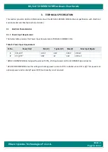
Power Input Requirement 

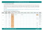
The below table provides the Power Input Requirement of RZ/G1E SODIMM SOM. 

Table 8: Power Input Requirement 

Sl. No. 

Power Rail 

Min (V) 

Typical (V) 

Max(V) 

Max Input Ripple 

VIN_3V3¹ 

3.15V 

3.3V 

3.45V 

±50mV 

VCC_RTC

2


2.8V 

3V 

3.3V 

±20 mV 

¹ RZ/G1E SODIMM SOM


is designed to work with VIN_3V3 input power rail from SODIMM Edge connector.  

2

 RZ/G1E SODIMM SOM


uses this voltage as backup power source to RTC controller when VCC is off. This power is an 

optional power and can be left open if RTC functionality is not required. 


Summary of Contents for iW-RainboW-G22M

Page 1: ...REL1 2 Page 1 of 62 RZ G1E SODIMM SOM Hardware User Guide iWave Systems Technologies Pvt Ltd iW RainboW G22M RZ G1E SODIMM SOM Hardware User Guide...

Page 2: ...the document 1 2 14th Jan 2019 Substantive changes throughout the document with respect to RZ G1E R4 0 SOM PROPRIETARY NOTICE This document contains proprietary material for the sole use of the inten...

Page 3: ...rata and associated issues Trademarks All registered trademarks product names mentioned in this publication are the property of their respective owners and used for identification purposes only Certif...

Page 4: ...WiFi and Bluetooth Interface 17 2 6 RTC Controller 17 2 7 SODIMM PCB Edge Connector 18 2 7 1 Gigabit Ethernet 19 2 7 2 10 100 Ethernet Optional 19 2 7 3 USB 2 0 OTG Interface 20 2 7 4 USB 2 0 Host Int...

Page 5: ...ristics 55 3 2 1 Environmental Specification 55 3 2 2 Heat Sink 55 3 2 3 RoHS Compliance 56 3 2 4 Electrostatic Discharge 56 3 3 MechanicalCharacteristics 57 3 3 1 SODIMM SOM Mechanical Dimensions 57...

Page 6: ...SODIMM SOM Side View 57 Figure 10 SODIMM Module Insertion procedure 58 Figure 11 SODIMM Module Removing Procedure 58 Figure 12 RZ G1E SODIMM SOM Development Platform 61 List of Tables Table 1 Acronyms...

Page 7: ...form factor of 67 6mm x 37mm and provides the functional requirements for an embedded application A single ruggedized SODIMM connector provides the carrier board interface to carry all the I O signals...

Page 8: ...nterface with FIFO PCB Printed Circuit Board PWM Pulse Width Modulation QSPI Quad Serial Peripheral Interface RTC Real Time Clock SCIF Serial Communication Interface with FIFO SD Secure Digital SDHI S...

Page 9: ...ctional Input output Signal CMOS Complementary Metal Oxide Semiconductor Signal DIFF Differential Signal OD Open Drain Signal OC Open Collector Signal Power Power Pin PU Pull Up PD Pull Down NA Not Ap...

Page 10: ...GP6_14 In this signal CAN0_RX is the functionality which we are using and GP6_14 is the GPIO number If CPU pin has multiplexing option and selected as GPIO function then the signal name is mentioned a...

Page 11: ...16Mb Upgradable QSPI QSPI DU0 RGB LCD 24bpp x 1 SSI3 SSI4 I2S x 1 CAN0 CAN1 CAN x 2 HSCIF1 HSCIF23 UART with CTS RTS x 2 SCIF1 SCIF2 SCIF3 SCIF5 UART x 4 SCIF4 Debug UART I2C3 I2C5 I2C x 2 MSIOF0 MSI...

Page 12: ...nsceiver 10 100Mbps Ethernet PHY Transceiver Optional Wi Fi and Bluetooth Module1 RTC controller SODIMM PCB Edge Interfaces Gigabit Ethernet x 1 Port through On SOM Gigabit Ethernet PHY transceiver 10...

Page 13: ...DIMM SOM with EtherMAC support instead of VIN1 3 Since HSCIF2 interface TXD and RXD signals are shared between Wi Fi BT module and SODIMM Edge pins either one only can be used at a time By default Wi...

Page 14: ...n Renesas s RZ G1E CPU with built in Dual ARM Cortex A7 MPCore which can operate up to 1 GHz core The Block Diagram of RZ G1E CPU from Renesas s website is shown below for reference Figure 2 RZ G1E Si...

Page 15: ...ip ROM starts up the QSPI and SYS DMAC channel 1 and transfers the loader program previously stored in the SPI Flash to the on chip RAM via the QSPI controller After loader program is transferred the...

Page 16: ...onnector J1 is directly connected to the SDHI1 controller of the RZ G1E CPU It also supports card detect feature through RZ G1E GPIO GP3_31 The main power to Micro SD Card Connector is 3 3 Voltage The...

Page 17: ...ule is 3 3 Voltage Wi Fi BT module U2 is physically located on top side of the SOM as shown below Note Since SDHI1 interface is shared between Wi Fi BT module and SD Connector either one only can be u...

Page 18: ...pports Mechnical specification of JEDEC Standard 200pin DDR S O DIMM PCB edge connector The interfaces which are available at SODIMM Edge connector are explained in the following sections Figure 5 SOD...

Page 19: ...nsformer TG1G E001NZRL HALO 40 C to 85 C Gigabit Ethernet Discrete Transformer HX5008NL Pulse 40 C to 85 C RJ45 Magjack with two Green LED JK0654219NL Pulse 0 C to 70 C RJ45 Magjack with two Green LED...

Page 20: ...12 Mbps Low Speed 1 5 Mbps transfer RZ G1E CPU s USB0 OTG controller OTG controller can operate in Host or Function Peripheral mode The RZ G1E CPU s USB0 PHY output is directly connected to SODIMM Ed...

Page 21: ...capture module that supports YCbCr 422 data through the ITU R BT 601 ITU R BT 656 or ITU R BT 709 interface and RGB data through the ITUR BT 601 or ITU R BT 709 interface The VIN supports Vertical and...

Page 22: ...I4 of SSIU is used for I2S interface The RZ G1E CPU s serial sound interface SSI is a transceiver module designed to send or receive audio data interfacing with a variety of devices offering I2S forma...

Page 23: ...SCIF2 56 57 for SCIF3 117 118 for SCIF4 7 9 for SCIF5 38 74 75 102 103 for HSCIF1 and 96 98 99 100 101 for HSCIF2 on Table 6 Note Since HSCIF2 interface TXD and RXD signals are shared between Wi Fi BT...

Page 24: ...1E CPU s TPU Time Pulse Unit is used for PWM interface which supports up to four channels in which TPUTO0 TPUTO2 and TPUTO3 channels are used in PWM mode This PWM timer has a 16 bit timers and support...

Page 25: ...efer SODIMM Edge connector pins 191 193 195 197 199 on Table 6 2 7 16 Power Input The RZ G1E SODIMM SOM works with single 3 3V power input VCC from SODIMM Edge connector and generates all other requir...

Page 26: ...XP NA IO DIFF Gigabit Ethernet differential pair 2 positive 9 SCIF5_TXD GP5_2 SSI_WS0129 AA7 O 3 3V CMOS SCIF5 Serial communication Interface data transmitter Note Same signal is optionally connected...

Page 27: ...GPIO GP0_16 1 A0 MD3 F4 IO 3 3V CMOS 10K PD General Purpose Input Output 29 GPIO GP0_17 1 A1 MD0 F3 IO 3 3V CMOS 100K PU General Purpose Input Output 30 NC NA Default NC Note Ethernet speed status LED...

Page 28: ...Power Ground 42 GPIO GP0_18 1 A2 MDT1 G4 IO 3 3V CMOS 10K PD General Purpose Input Output 43 GPIO GP1_10 CS0 E2 IO 3 3V CMOS General Purpose Input Output Note GP0_20 is optionally connected to this pi...

Page 29: ...GP4_22 I2C2_SCL AD21 IO 3 3V CMOS General Purpose Input Output 59 GPIO GP4_23 I2C2_SDA AC20 IO 3 3V CMOS General Purpose Input Output 60 VIN_3V3 NA I 3 3V Power Supply Voltage 61 SSI_SDATA4 GP5_9 SSI...

Page 30: ...ansmission and reception 74 HSCIF1_HSCK GP4_10 HSCIF1_HSCK AA24 IO 3 3V CMOS HSCIF1 High Speed Serial Communication Interface clock Or General Purpose Input Output 75 HSCIF1_HRTS GP4_12 HSCIF1_HRTS AB...

Page 31: ...ord select 93 ETH_TXD1 VI1_DATA5 GP 5_17 SSI_SCK9 AE3 I 3 3V CMOS VIN1 Parallel camera data 05 Note GP1_16 is optionally connected to this pin through resistor and default not populated 94 SCIF1_TXD G...

Page 32: ...1 High Speed Serial Communication Interface serial data receiver 104 ETH_REF_CLK VI1_DATA4 GP5_16 SSI_SDATA2 AC4 I 3 3V CMOS VIN1 Parallel camera data 4 Note GP1_17 is optionally connected to this pin...

Page 33: ...AC2 I 3 3V CMOS VIN1 Parallel camera VSYNC 122 GPIO GP1_22 1 WE1 MD20 L4 IO 3 3V CMOS 10K PD General Purpose Input or Output Note CLKOUT from CPU is optionally connected to this pin through resistor a...

Page 34: ...for VBUS supply 141 NC NA Default NC Note GP4_0 is optionally connected to this pin through resistor and default not populated Note Same signal is by default connected to SODIMM edge connector 48th pi...

Page 35: ...VIN_3V3 NA I 3 3V Power Supply Voltage 161 DU0_DG3 GP2_11 DU0_DG3 AD16 O 3 3V CMOS 10K PD DU0 Parallel LCD data 11 Green data3 162 DU0_DG4 GP2_12 DU0_DG4 AB17 O 3 3V CMOS DU0 Parallel LCD data 12 Gre...

Page 36: ...O 3 3V CMOS 10K PD MSIOF2 frame synchronization signal2 182 GPIO GP1_14 EX_CS2 D1 I 3 3V CMOS General Purpose Input Output 183 VRTC_3V0 NA I 3V Power 3V backup coin cell input for RTC 184 GPIO GP4_1 I...

Page 37: ...receive data 197 TCK TCK N22 I 3 3V CMOS JTAG Test Clock 198 GND NA Power Ground 199 TMS TMS P21 I 3 3V CMOS JTAG Test Mode Select 200 NC NA NC Note Recommending to connect always available 5V to this...

Page 38: ...gly recommended to use the pin function same as selected in the SODIMM SOM Edge connector for iWave s BSP reusability and to have compatible SODIMM modules in future for upgradability Table 7 RZ G1E C...

Page 39: ...D_B IIC0_SDA_C VI1_DATA0 CAN0_TX_D ETH_RX_ER_B GP5_12 GP5_12 70 AE4 SI_SCK2 HSCIF1_HTX_ B VI1_DATA2 ATAG0 ETH_RXD 1_B GP5_14 GP5_14 93 AE3 SSI_SCK9 SCIF2_SCK_B PWM2_B VI1_DATA5 EX_WAIT 1 ETH_TXD1_B GP...

Page 40: ...SYNC GP2_27 GP2_27 145 AE14 DU0_DOTCLK OUT0 GP2_25 GP2_25 146 AE18 DU0_DISP GP2_30 GP2_30 148 AA18 DU0_DR0 SCIF5_RXD_C I2C2_SCL_D GP2_0 GP2_0 149 AB18 DU0_DR1 SCIF5_TXD_C I2C2_SDA_D GP2_1 GP2_1 150 AE...

Page 41: ...nction 8 GPIO Default State 163 AA16 DU0_DG5 GP2_13 GP2_13 164 AE16 DU0_DG6 GP2_14 GP2_14 165 AC16 DU0_DG7 GP2_15 GP2_15 166 AC14 DU0_DB0 SCIFA4_RXD_C I2C4_SCL_D CAN0_RX_C GP2_16 GP2_16 167 AE17 DU0_D...

Page 42: ...SCIFA1_SCK_C DREQ1 _B GP5_4 GP5_4 91 AD22 SSI_SCK4 GP5_7 GP5_7 92 AB21 SSI_WS4 GP5_8 GP5_8 CAN0 176 AD8 SD1_CD CAN0_RX GP6_14 GP6_14 178 AE9 SD1_WP IRQ7 CAN0_TX GP6_15 GP6_14 CAN1 175 K4 A17 MSIOF2_SY...

Page 43: ...P5_1 GP5_1 9 AA7 SSI_WS0129 MSIOF1_TXD _B SCIF5_TXD_D GP5_2 GP5_2 Debug UART 118 B4 D6 SCIF4_TXD_B I2C0_SDA_D GP0_6 GP0_6 117 C5 D5 SCIF4_RXD_B I2C0_SCL_D GP0_5 GP0_5 HSCIF1 38 Y23 HSCIF1_HCTS SCIFA4_...

Page 44: ...MSIOF0_SYN C PWM1 DU1_DR5 GP4_5 GP4_5 MSIOF1 47 H3 A11 MSIOF1_SYN C GP0_27 GP0_27 71 G1 A13 MSIOF1_SS2 GP0_29 GP0_29 MSIOF2 181 K3 A19 MSIOF2_SS2 PWM4 TPUTO2 GP1_3 GP1_3 189 J2 A16 MSIOF2_SCK HSCIF0_H...

Page 45: ...AA6 SSI_SDATA0 MSIOF1_SCK PWM0_B GP5_3 GP5_3 25 C2 EX_WAIT0 CAN_CLK_B SCIF_CLK GP1_23 GP1_23 26 L5 DREQ0 SCIFB1_RXD GP1_24 GP1_24 28 F4 A0 SCIFB1_SCK PWM3_B GP0_16 GP0_16 29 F3 A1 SCIFB1_TXD GP0_17 G...

Page 46: ...DU1_CDE GP4_31 GP4_31 129 AB19 SSI_SCK78 SCIFA2_SCK_ B I2C5_SDA_C DU1_DISP GP4_30 GP4_30 130 AA20 SSI_SDATA5 SCIFA3_TXD I2C3_SDA_C DU1_DOTCL KOUT1 GP4_26 GP4_26 132 AE20 SSI_SCK6 SCIFA1_SCK_ B DU1_HSY...

Page 47: ...F_SCK IIC0_SCL_B GP0_26 70 G2 A9 MSIOF_TXD SCIFA0_TXD_B GP0_25 GPIOs Optional 93 C1 EX_CS4 SCIFA2_RXD I2C2_SCL_E SCIFB2_CTS GP1_16 104 B2 EX_CS5 SCIFA2_TXD I2C2_SDA_E SCIFB2_RTS GP1_17 110 M3 RD ATACS...

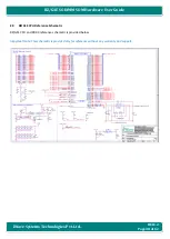
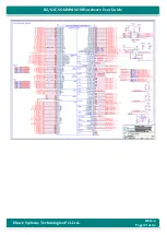
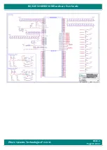
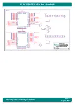
Page 48: ...ologies Pvt Ltd RZ G1E SODIMM SOM Hardware User Guide 2 9 RZ G1E CPU Reference Schematic RZ G1E CPU and DDR3 reference schematic is provided below Important Note This schematic is provided only for re...

Page 49: ...REL1 2 Page 49 of 62 iWave Systems Technologies Pvt Ltd RZ G1E SODIMM SOM Hardware User Guide...

Page 50: ...REL1 2 Page 50 of 62 iWave Systems Technologies Pvt Ltd RZ G1E SODIMM SOM Hardware User Guide...

Page 51: ...REL1 2 Page 51 of 62 iWave Systems Technologies Pvt Ltd RZ G1E SODIMM SOM Hardware User Guide...

Page 52: ...nput Requirement The below table provides the Power Input Requirement of RZ G1E SODIMM SOM Table 8 Power Input Requirement Sl No Power Rail Min V Typical V Max V Max Input Ripple 1 VIN_3V3 3 15V 3 3V...

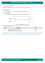
Page 53: ...Power down Sequence VIN_3V3 must go down at the same time or before VCC_RTC goes down Figure 6 SODIMM SOM Power Sequence Table 9 Power Sequence Timing Item Description Value T1 VCC_RTC rise time to VI...

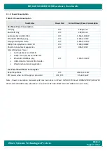
Page 54: ...9W 1080p Video playback on RGB LCD VCC 0 93A 3 069W Dhrystone benchmark application VCC 0 9A 2 97W Typical Maximum Power Audio playback on SSI3 SSI4 1080p Video playback on RGB LCD EtherAVB 1000Mbps p...

Page 55: ...before using this board in the end application If Micro SD connector is supported in RZ G1E SODIMM SOM then operating temperature range is 25 C to 85 C 3 To meet this humidity specification conformal...

Page 56: ...g RoHS compliant components and manufactured on lead free production process 3 2 4 Electrostatic Discharge iWave s RZ G1E SODIMM SOM is sensitive to electro static discharge and so high voltages cause...

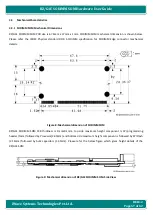
Page 57: ...d DDR S O DIMM specification for SODIMM Edge connector mechanical details Figure 8 Mechanical dimension of SODIMM SOM RZ G1E SODIMM SOM PCB thickness is 1mm 0 1mm top side maximum height component is...

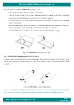
Page 58: ...ward as indicated in the illustration Continue pressing downward until the clips at each end of the socket lock into position Once the SOM have been installed Carrier board can be Powered ON with 5V p...

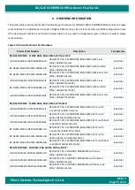
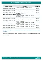
Page 59: ...1E PF CPU 512MB DDR3 8GB eMMC with Android Ether AVB Ether MAC Industrial iW G22M SM02 3D512M E008G BIE RZ G1E PF CPU 512MB DDR3 8GB eMMC with boot code Ether AVB Ether MAC Industrial RZ G1E SODIMM 51...

Page 60: ...SM02 3D002G E008G AIF RZ G1E PF CPU 2GB DDR3 8GB eMMC Wi Fi with Android Ether AVB Camera Industrial iW G22M SM02 3D002G E008G BIF RZ G1E PF CPU 2GB DDR3 8GB eMMC Wi Fi with boot code Ether AVB Camer...

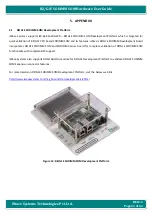
Page 61: ...iWave s RZ G1E SODIMM Development Board incorporates RZ G1E SODIMM SOM and SODIMM Carrier board for complete validation of RZ G1E SODIMM SOM functionality with complete BSP support iWave Systems also...

Page 62: ...REL1 2 Page 62 of 62 iWave Systems Technologies Pvt Ltd RZ G1E SODIMM SOM Hardware User Guide...

Reviews: