REL1.1
Page 24 of 51
iWave Systems Technologies Pvt. Ltd.
RZ/G1C SBC Hardware User Guide
2.8.2
SPI Flash Programming Header
To program the boot code in to the SPI flash (for the first time or if boot code is corrupted),
use iWave’s
RZ/G1C SPI
Programmer Board through 6pin SPI Flash Programming Header (J6) (or) JTAG debugger through JTAG Header (J14).
Optionally the external SPI programmer can be used for programming the SPI flash through SPI Flash Programming
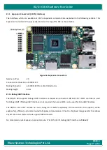
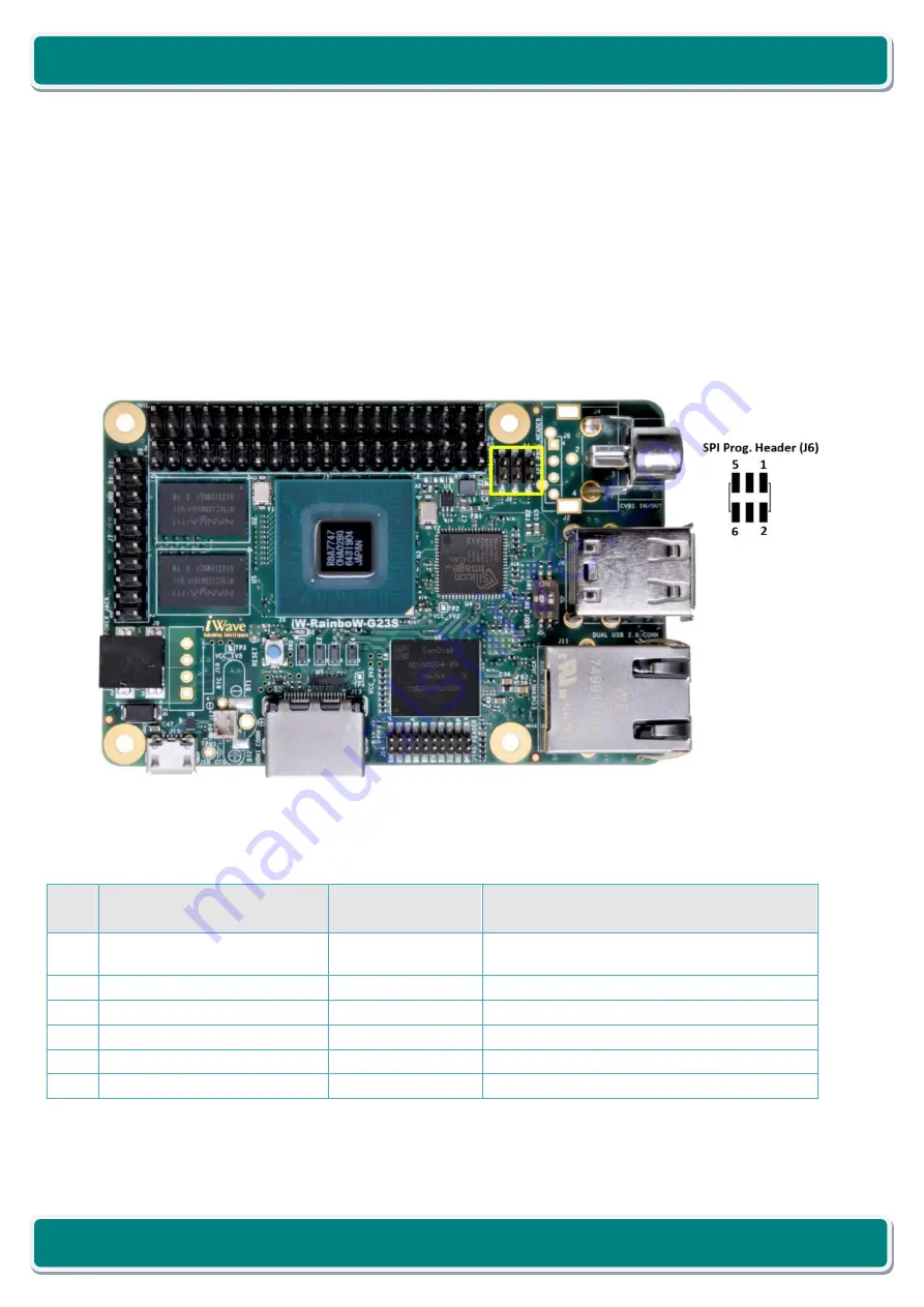
Header (J6). The 6pin SPI Flash Programming Header is physically located on top side of the SBC as shown below.
Number of Pins
- 6
Connector Part Number - 87759-0614
Mating Connector
- 79107-7002 from Molex
Figure 11: SPI Flash Programming Header
Table 5: SPI Flash Programming Header Pin Assignment
Pin
No.
Signal Name
Signal Type/
Termination
Description
1
SPI_CS
I, 3.3V CMOS/
10K PU
SPI Flash Chip Select.
2
SPI_SO
O, 3.3V CMOS
SPI Flash Serial Data Output.
3
GND
Power
Ground
4
SPI_SI
I, 3.3V CMOS
SPI Flash Serial Data Input.
5
SPI_SCK
I, 3.3V CMOS
SPI Flash Serial clock.
6
VCC_3V3
O, 3.3V Power
3.3V Power Supply.


