background image


REL1.1 

Page 32 of 51 

iWave Systems Technologies Pvt. Ltd. 

RZ/G1C SBC Hardware User Guide


2.10


Expansion Connector2 (40 Pin) Interfaces 

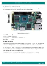
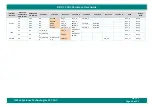
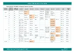
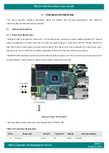
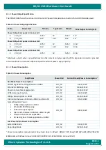
The  interfaces  which  are  available  at  40  Pin  Expansion  connector2  are  explained  in  the  following  sections.  This 

Expansion Connector2 (J3) is physically located at the top of the SBC as shown below. 


Figure 15: Expansion Connector2 

Number of Pins  

- 40 

Connector Part Number - 61304021121 

Mating Connector 

- 61304021821 from Wurth Electronics 

Staking Height    

- 6mm 


Summary of Contents for iW-RainboW-G23S

Page 1: ...REL1 1 Page 1 of 51 iWave Systems Technologies Pvt Ltd RZ G1C SBC Hardware User Guide iW RainboW G23S RZ G1C Single Board Computer Hardware User Guide...

Page 2: ...NOTICE This document contains proprietary material for the sole use of the intended recipient s Do not read this document if you are not the intended recipient Any review use distribution or disclosur...

Page 3: ...and associated issues Trademarks All registered trademarks product names mentioned in this publication are the property of their respective owners and used for identification purposes only Certificat...

Page 4: ...ication Features 18 2 6 1 100 1000 Mbps Ethernet Port 18 2 6 2 Dual USB 2 0 Host Ports 19 2 6 3 USB 2 0 Device Port 20 2 7 Video Features 21 2 7 1 HDMI Port 21 2 7 2 CVBS Input Port 22 2 7 3 CVBS Outp...

Page 5: ...C Pin Multiplexing on Expansion Connectors 40 3 TECHNICAL SPECIFICATION 45 3 1 Electrical Characteristics 45 3 1 1 Power Input Requirement 45 3 1 2 Power Output Specification 46 3 1 3 Power Consumptio...

Page 6: ...Dimension of RZ G1C SBC Top View 48 Figure 19 Mechanical Dimension of RZ G1C SBC Side View 48 Figure 20 RZ G1C SPI Programmer Board 50 List of Tables Table 1 Acronyms Abbreviations 7 Table 2 Terminol...

Page 7: ...and provides the functional requirements for an embedded application 1 3 List of Acronyms The following acronyms will be used throughout this document Table 1 Acronyms Abbreviations Acronyms Abbreviat...

Page 8: ...ulation QSPI Quad Serial Peripheral Interface RTC Real Time Clock SBC Single Board Computer SCIF Serial Communication Interface with FIFO SD Secure Digital SDHI SD Card Host Interface SSI Serial Sound...

Page 9: ...ectional Input output Signal CMOS Complementary Metal Oxide Semiconductor Signal DIFF Differential Signal LVDS Low Voltage Differential Signal OD Open Drain Signal OC Open Collector Signal Power Power...

Page 10: ...In this signal CAN0_RX is the functionality which we are using and GP0_11 is the GPIO number If CPU pin has multiplexing option and selected as GPIO function then the signal name is mentioned as GPIO...

Page 11: ...AG SPI Flash 16MB Upgradable SPI Reset QSPI0 JTAG USB0 USB MicroB Connector 40Pin Expansion Connector2 LVDS CAN0 I2C3 HSCIF1 2 SCIF5 SSI0 9 1 PWM0 Power IN Jack Optional 4Pin Lockable Header Power to...

Page 12: ...pandable Micro SD Connector Communication Features 100 1000 Mbps Ethernet through RJ45 MagJack 1 USB2 0 Host x 2 Ports through Dual Stack Type A Connector USB2 0 OTG as Device x 1 Port through MicroB...

Page 13: ...8bit x 1 Port 1 PWM x 1 General Specification Power Input Jack 5V 2 5A Power Input Lockable Header Optional Form Factor 85mm x 56mm 1 In RZ G1C CPU EtherAVB collision detection signal and VIN0 clock...

Page 14: ...sas s RZ G1C CPU with built in Dual ARM Cortex A7 MPCore which can operate up to 1 GHz core The Block Diagram of RZ G1C CPU from Renesas s website is shown below for reference Figure 2 RZ G1C CPU Simp...

Page 15: ...is physically located in the top of the PCB This switch is used to select the boot media of RZ G1C CPU RZ G1C SBC supports two boot media options for booting RZ G1C CPU as mentioned in the below table...

Page 16: ...sly stored in the SPI Flash to the on chip RAM via the QSPI controller After loader program is transferred the program automatically jumps to the top address of the loader program The SPI flash memory...

Page 17: ...and UHS I SDR50 transfer modes upto 78 MHz It also supports card detect feature through RZ G1C GPIO GP4_20 The main power to Micro SD Card Connector is 3 3 Voltage The RZ G1C SBC supports configurabl...

Page 18: ...therAVB interface The MAC is integrated in the RZ G1C CPU and connected to the external Gigabit Ethernet PHY KSZ9031MNX The Gigabit Ethernet PHY output is directly to connected to RJ45 Magjack J11 RZ...

Page 19: ...RZ G1C CPU s USB1 controller is interfaced with two port USB hub USB2422 This Hub output port1 port2 is connected to USB Type A Dual stack connector J8 This Dual Stack Connector J8 is physically loca...

Page 20: ...B0 controller with integrated PHY which supports USB2 0 High Speed 480 Mbps Full Speed 12 Mbps Low Speed 1 5 Mbps transfer is directly connected to USB Micro B Connector J15 and used in Function Perip...

Page 21: ...nsion Conenctor2 and optionally one CVBS output interface on RCA Jack Upon these three interfaces either two interfaces can be used at a time The RZ G1C SBC supports HDMI output through on board RGB t...

Page 22: ...support CVBS input signal and directly connects to the RZ G1C CPU s VIN1A input This CVBS IN RCA Jack J4 is physically located at the top of the SBC as shown below Figure 9 CVBS IN RCA Jack 2 7 3 CVB...

Page 23: ...for backup battery coincell connection In SBC power off condition RTC controller will take power from RTC battery coincell power and continues to keep the current time The 2pin RTC battery connector i...

Page 24: ...e 6pin SPI Flash Programming Header is physically located on top side of the SBC as shown below Number of Pins 6 Connector Part Number 87759 0614 Mating Connector 79107 7002 from Molex Figure 11 SPI F...

Page 25: ...20 connector the physical dimension of connector is made smaller in RZ G1C SBC because of space constraint RZ G1C CPU s JTAG pins are 1 8V tolerant and so 1 8V reference power is provided to pin 1 of...

Page 26: ...ound 5 JTAG_TDI JTAG_TDI I 1 8V CMOS 4 7K PU JTAG test data Input 6 GND GND Power Ground 7 JTAG_TMS JTAG_TMS I 1 8V CMOS 4 7K PU JTAG test mode select 8 GND GND Power Ground 9 JTAG_TCK JTAG_TCK I 1 8V...

Page 27: ...s Pvt Ltd RZ G1C SBC Hardware User Guide 2 8 4 Reset Switch The RZ G1C SBC supports Push button switch SW2 to reset the RZ G1C CPU This Reset Push button switch SW2 is physically located at the top of...

Page 28: ...sion connectors and one 20 pin Expansion Connector The interfaces which are available at 40 Pin Expansion connector1 are explained in the following sections This Expansion Connector1 J1 is physically...

Page 29: ...sion connector1 pins 19 21 23 24 26 pins for MSIOF2 on Table 7 2 9 3 I2C Interface The RZ G1C SBC supports two I2C interface on Expansion connector1 RZ G1C CPU s I2C1 I2C4 channels are used for I2C in...

Page 30: ...CMOS General purpose input output 8 SCIF2_TX2_B GP5_26 SSI_WS9_A K2 O 3 3V CMOS SCIF2 Serial Communication Interface Serial Data Transmitter 9 GND NA Power Ground 10 SCIF2_RX2_B GP5_25 SSI_SCK9_A K3...

Page 31: ...3 3V CMOS General purpose input output Note The same signal can also be used as PWM6 30 GND NA Power Ground 31 GPIO GP4_7 MSIOF0_SYNC_ A B5 IO 3 3V CMOS General purpose input output 32 GPIO GP1_15 D1...

Page 32: ...rfaces which are available at 40 Pin Expansion connector2 are explained in the following sections This Expansion Connector2 J3 is physically located at the top of the SBC as shown below Figure 15 Expa...

Page 33: ...bit rate up to 1 Mbps with both formats of messages namely the standard identifier 11 bits and extended ID 29 bits It also supports 64 mailboxes in two selectable mailbox mode Normal mailbox mode and...

Page 34: ...fast efficient and uninterrupted communication For more details refer Expansion connector2 pins 28 30 for SCIF5 32 34 36 38 for HSCIF1 and 18 20 22 24 26 for HSCIF2 on Table 8 2 10 5I2C Interface The...

Page 35: ...3 3V LVDS LVDS data output3 negative 10 SSI_WS0129_B GP0_9 SD0_DAT2 C14 IO 3 3V CMOS Audio Word select for SSI channel 0 11 GND NA Power Ground 12 SSI_SDATA9_B GP4_21 SD2_WP D8 IO 3 3V CMOS Audio Seri...

Page 36: ...data output0 positive 32 HSCIF1_HCTS1_A GP4_12 HCTS1 _A E8 I 3 3V CMOS High Speed Serial Communication Interface HSCIF1 Clear to Send 33 TXOUT0M TXOUT0M AE13 O 3 3V LVDS LVDS data output0 negative 34...

Page 37: ...lectronics Staking Height 6mm 2 11 1Debug UART Interface The RZ G1C SBC supports Debug UART interfaces on Expansion connector3 RZ G1C CPU s SCIF1 controller is used for Debug UART If Debug UART interf...

Page 38: ...e RZ G1C CPU s Video Input Module VIN0 is a video capture module that supports YCbCr 422 data through the ITU R BT 601 ITU R BT 656 or ITU R BT 709 interface and RGB data through the ITUR BT 601 or IT...

Page 39: ...V Power Supply 7 PWM2_D GP5_27 SSI_SDATA9_A K1 O 3 3V CMOS Pulse Width Modulated output 2 8 VI0_G2 GP4_4 MSIOF0_RXD_A A6 I 3 3V CMOS Video Input0 Data 2 9 VI0_G4 GP4_6 MSIOF0_SCK_A A5 I 3 3V CMOS Vide...

Page 40: ...nterfaces Interface Function Expansion Connnector1 Pin Numbers RZ G1C CPU Pin Number Function 1 Function 2 Function 3 Function 4 Function 5 Function 6 Function 7 Function 8 GPIO Default State SCIF2 8...

Page 41: ...ATA7_ B GP4_7 GP4_7 33 E3 AUDIO_CLKB _A SDA0_B Reserved TANS2 VI0_FIELD GP5_29 GP5_29 35 C4 SDA2_A MSIOF1_SYN C_B DU1_DB7 AUDIO_CLKO UT_C GP4_25 GP4_25 37 B4 SCL2_A MSIOF1_SCK _B DU1_DB6 AUDIO_CLKC _C...

Page 42: ...SD0_WP IRQ7 CAN0_TX_A GP0_12 GP0_12 14 A8 SD0_CD CAN0_RX_A GP0_11 GP0_11 SSI1 1 A13 SD0_CLK SSI_SCK1_C RX3_C GP0_5 GP0_5 3 B13 SD0_DAT0 SSI_SDATA1_ C RX4_E GP0_7 GP0_7 5 D13 SD0_CMD SSI_WS1_C TX3_C G...

Page 43: ...Default State HSCIF2 18 AA3 D8 HCTS2 RX1_C SCL1_D PWM3_C GP1_8 GP1_8 20 AA2 D9 HRTS2 TX1_C SDA1_D GP1_9 GP1_9 22 AB2 D5 HRX2 SCL1_B PWM2_C TCLK2_B Reserved GP1_5 GP1_5 24 AB1 D6 HTX2 SDA1_B PWM4_C Res...

Page 44: ...CON_ A DACK2 VI0_CLK AVB_COL GP5_18 GP5_18 2 E4 AUDIO_CLKC _A SCL4_B Reserved VI0_HSYNC GP5_30 GP5_30 3 E1 AUDIO_CLKO UT_A SDA4_B Reserved VI0_VSYNC GP5_31 GP5_31 4 E2 AUDIO_CLKA _A SCL0_B Reserved TA...

Page 45: ...xternal power supply is connected to the SBC through Power Jack J9 This 1 3mm x 3 9mm barrel connector Jack should fit DC Plugs with an inner dimension of 1 3mm and an outer dimension of 3 4mm This Po...

Page 46: ...y 3 1 3 Power Consumption Table 15 Power Consumption Task Status Power Rail Current Drawn Power Consumption Run Mode Power Consumption 3D Gaming bench mark application on HDMI VCC_5V 0 42A 2 1W EtherA...

Page 47: ...recommended to do the necessary system level thermal simulation and find necessary thermal solution in the system before using this board in the end application If CVBS Input RCA Jack is not supporte...

Page 48: ...s shown below Figure 18 Mechanical Dimension of RZ G1C SBC Top View RZ G1C SBC PCB thickness is 1 6mm 0 1mm top side maximum height connector is Dual USB Stack connector 15 91mm followed by Ethernet c...

Page 49: ...if any custom configuration part number is required please contact iWave Table 17 Orderable Product Part Numbers Product Part Number Description Temperature RZ G1C Dual Core CPU based SBC iW G23S CC0...

Page 50: ...n to the RZ G1C SBC s SPI flash through 6pin SPI Flash Programming Header J6 This RZ G1C SPI Programmer Board has single bit DIP switch to select the SPI Flash chip select The RZ G1C SPI Programmer Bo...

Page 51: ...REL1 1 Page 51 of 51 RZ G1C SBC Hardware User Guide iWave Systems Technologies Pvt Ltd...

Reviews: