REL1.1
Page 30 of 51
iWave Systems Technologies Pvt. Ltd.
RZ/G1C SBC Hardware User Guide
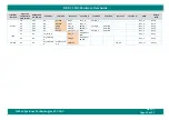
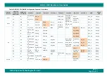
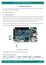
Table 7: Expansion Connector1 Pin Assignment
Pin
No.
Signal Name
CPU Ball Name/
Pin Number
Signal Type/
Termination
Description
1
VCC_3V3
NA
O, 3.3V Power
3.3V Power Supply.
2
VCC_5V
NA
O, 5V Power
5V Power Supply.
3
I2C4_SDA(GP5_6)
SSI_SCK78_A/
D3
IO, 3.3V OD/
1K PU
I2C4 Data.
Note: I2C4_SDA is connected to this Pin
through resistor and default populated.
Note: Same I2C4 is also connected to On-
board HDMI transmitter.
4
VCC_5V
NA
O, 5V Power
5V Power Supply.
5
I2C4_SCL(GP5_7)
SSI_WS78_A/
D2
O, 3.3V OD/
1K PU
I2C4 Clock.
Note: I2C4_SCL is connected to this Pin
through resistor and default populated.
Note: Same I2C4 is also connected to On-
board HDMI transmitter.
6
GND
NA
Power
Ground.
7
GPIO(GP0_4)
CLKOUT/
AE2
IO, 3.3V CMOS
General purpose input/output.
8
SCIF2_TX2_B(GP5_26)
SSI_WS9_A/
K2
O,3.3V CMOS
SCIF2 Serial Communication Interface
Serial Data Transmitter.
9
GND
NA
Power
Ground.
10
SCIF2_RX2_B(GP5_25)
SSI_SCK9_A/
K3
I, 3.3V CMOS
SCIF2 Serial Communication Interface
Serial Data Receiver.
11
GPIO(GP4_8)
MSIOF0_SS1_A/
C6
IO, 3.3V CMOS
General purpose input/output.
12
GPIO(GP4_9)
MSIOF0_SS2_A/
D6
IO, 3.3V CMOS
General purpose input/output.
13
GPIO(GP5_15)
SSI_SCK4_A/
G4
IO, 3.3V CMOS
General purpose input/output.
14
GND
NA
Power
Ground.
15
GPIO(GP5_21)
SSI_SDATA1_A/
J4
IO, 3.3V CMOS
General purpose input/output.
16
GPIO(GP2_26)
DU0_DOTCLKO
UT1/AB11
IO, 3.3V CMOS
General purpose input/output.
17
VCC_3V3
NA
O, 3.3V Power
3.3V Power Supply.
18
GPIO(GP1_22)
EX_WAIT0/
AE3
IO, 3.3V CMOS
General purpose input/output.
19
MSIOF2_TXD_A(GP1_11)
D11/
Y5
O,3.3V CMOS
SPI Master serial output/Slave serial
input (MSIOF2).
20
GND
NA
Power
Ground.
21
MSIOF2_RXD_A(GP1_10)
D10/
AA1
I,3.3V CMOS
SPI Master serial input /Slave serial
output (MSIOF2).


