REL0.1
Page 12 of 95
Kintex Ult FPGA SOM Hardware User Guide
iWave Systems Technologies Pvt. Ltd.
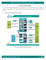
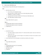
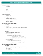
FPGA to CPU Interfaces
•
PCIex1 Gen2
•
RGMII
•
UART
•
Slide IDs
•
Interrupt Request Pins
Other On-SOM Features
•
TPM 2.0 Module
•
Temperature Sensor
•
Gigabit Ethernet PHY Transceiver
•
Clock Synthesizer for On-SOM Clocks
•
Fan Header (Optional)
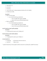
Board to Board
Connector1
I
nterfaces (240pin)
From LS1021a
•
USB 3.0 x 1
•
1 SerDes lane for high-speed peripheral interface with reference clock
•
6 GPIOs From LS1021A
From KU19P
•
GTY High Speed Transceivers (up to 32.75Gbps) x 8
•
FPGA IOs - HD Bank 92
➢
Up to 11 LVDS IOs/22 Single ended (SE) IOs
o
Up to 3 HDGC Global Clock Input pins (LVDS/SE)
o
Up to 11 ADC Input pins (Differential/Single Ended)
•
FPGA IOs - HP Bank 65,67
➢
Up to 5 LVDS IOs/14 Single ended (SE) IOs
o
Up to 4 HDGC Global Clock Input pins (LVDS/SE)
Board to Board Connector2 Interfaces (240pin)
From LS1021a
•
Gigabit Ethernet x 1 Port (through On-SOM Gigabit Ethernet PHY)
•
USB2.0 x 1 Port
•
Debug UART x 1 Port


