REL0.1
Page 25 of 95
Kintex Ult FPGA SOM Hardware User Guide
iWave Systems Technologies Pvt. Ltd.
2.5.3
UART
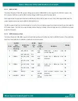
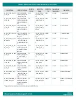
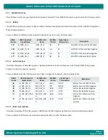
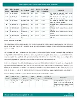
The Kintex Ult SOM supports UART interface between LS1021A Processor and KU19P through LPUART6 of LS1021A
Processor and FPGA HP Bank65 of KU19P. Refer the below table for more details.
Signal Name
LS1021A Pin Name
LS1021A
Pin No
KU19P Pin Name
KU19P
Pin No.
Signal Type/
Termination
*
Description
LS_LPUART6_SO
UT_PL_AY25_L1
0N_65
SDHC_DAT3/GPIO2
_08/LPUART3_RTS
_B/LPUART6_SOUT
G1
IO_L10N_T1U_N7_
QBC_AD4N_A13_D
29_65
AY25
O, 1.8V
Transmit Data
LS_LPUART6_SI
N_PL_AW25_L1
0P_65
SDHC_CLK/GPIO2_
09/LPUART3_CTS_
B/LPUART6_SIN
D1
IO_L10P_T1U_N6_
QBC_AD4P_A12_D
28_65
AW25
I, 1.8V
Receive Data
*
Signal type is mentioned with respect to LS1021A processor
2.5.4
Interrupt Request pins
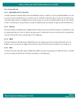
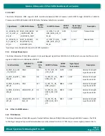
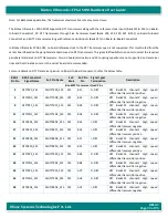
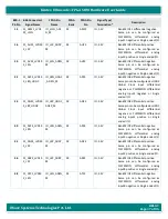
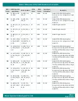
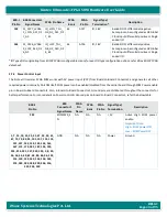
The Kintex Ult FPGA SOM supports 4 Interrupt Request signals from LS1021A to KU19P, which is connected from control
signals of LS1021A to PL HP Bank 65 of KU19P.
Function Name
LS1021A Pin
Name
LS1021
A Pin
No
KU19P Pin Name
KU19P
Pin No.
Signal Type/
Termination
Description
LS_IRQ0_PL_AU25
_CSI_ADV_65
IRQ0
G6
IO_T2U_N12_CSI
_ADV_B_65
AU25
I, 1.8V
External Interrupt0
input from KU19P
LS_IRQ1_PL_BB27_
L8N_65
IRQ1
G8
IO_L8N_T1L_N3_
AD5N_A17_65
BB27
I, 1.8V
External Interrupt1
input from KU19P
LS_IRQ2_PL_BB26_
L8P_65
IRQ2
W7
IO_L8P_T1L_N2_
AD5P_A16_65
BB26
I, 1.8V
External Interrupt2
input from KU19P
LS_IRQ3_PL_BA28_
L9N_65
IRQ3/GPIO1_23
R5
IO_L9N_T1L_N5_
AD12N_A15_D31
_65
BA28
I, 1.8V
External Interrupt3
input from KU19P
LS_IRQ4_PL_BA27_
L9P_65
IRQ4/GPIO1_24/S
DHC_VS
L2
IO_L9P_T1L_N4_
AD12P_A14_D30
_65
BA27
I, 1.8V
External Interrupt4
input from KU19P
2.6
Other On SOM Features
2.6.1
TPM Module
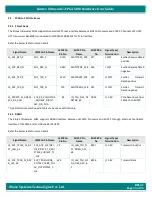
The Kintex Ult FPGA SOM supports Trusted Platform Module (TPM) 2.0 Module through LS1021A Processor. The TPM
technology is designed to provide hardware-based, security-related functions. A TPM chip is a secure crypto-processor that is

