REL0.1
Page 31 of 95
Kintex Ult FPGA SOM Hardware User Guide
iWave Systems Technologies Pvt. Ltd.
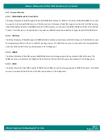
2.7.1
LS1021A Interfaces
The interfaces which are supported in Board-to-Board Connector1 from LS1021A Processor is explained in the following section
2.7.1.1
USB3.0
The LS1021A Layerscape processor supports USB3.0 interface through Board-to-Board Connector1 from USB PHY integrated in
the Layerscape processor.
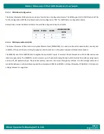
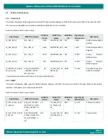
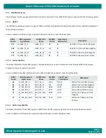
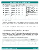
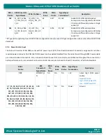
For more details on USB3.0 pinouts on Board-to-Board Connector1, refer the below table.
B2B-1
Pin No
B2B Connector1
Signal Name
LS1021A Pin
Name
LS1021A
Pin No
Signal Type/
Termination
Description
157
LS_USB1_TX_P
USB1_TX_P
B2
IO
USB PHY 3.0 Transmit Data Positive
159
LS_USB1_TX_M
USB1_TX_M
A2
IO
USB PHY 3.0 Transmit Data Negative
175
LS_USB1_RX_M
USB1_RX_M
A4
IO
USB PHY 3.0 Receive Data Negative
177
LS_USB1_RX_P
USB1_RX_P
B4
IO
USB PHY 3.0 Receive Data Positive
2.7.1.2
SerDes Interface
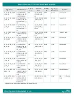
The Kintex Ult FPGA SOM supports 1 highspeed SerDes lane and its reference clock through LS1021A Layerscape
Processor in board-to-board connector1
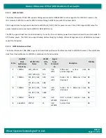
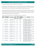
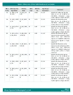
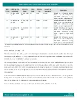
For more details on SerDes Interface pinouts on Board-to-Board Connector1, refer the below table.
B2B-2
Pin No
B2B Connector1
Signal Name
LS1021A Pin
Name
LS1021A
Pin No
Signal Type/
Termination
Description
63
LS_SD1_TX2_P
SD1_TX2_P
W13
O, DIFF
SerDes Transmit Data Positive
65
LS_SD1_TX2_N
SD1_TX2_N
Y13
O, DIFF
SerDes Transmit Data Negative
81
LS_SD1_RX2_N
SD1_RX2_N
AB13
I, DIFF
SerDes Receive Data Negative
83
LS_SD1_RX2_P
SD1_RX2_P
AC13
I, DIFF
SerDes Receive Data Positive
75
LS_SD1_REF_CLK2_
N
SD1_REF_CLK2_
N
AB16
I, DIFF
SerDes PLL 2 Reference Clock
Negative
77
LS_SD1_REF_CLK2_
P
SD1_REF_CLK2_
P
AC16
I, DIFF
SerDes PLL 2 Reference Clock
Positive
2.7.1.3
GPIOs From LS1021A
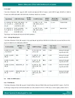
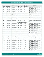
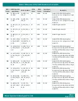
The Kintex Ult FPGA SOM supports 6 GPIOs from LS1021A Layerscape Processor in board-to-board connector1
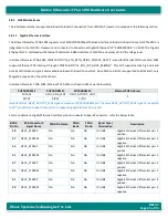
For more details on GPIOs pinouts on Board-to-Board Connector2, refer the below table.

