REL0.1
Page 39 of 95
Kintex Ult FPGA SOM Hardware User Guide
iWave Systems Technologies Pvt. Ltd.
B2B-1
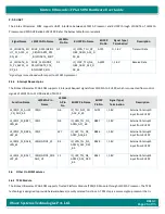
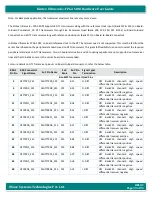
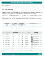
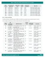
Pin No
B2B Connector1
Signal Name
FPGA Pin Name
FPGA
Bank
FPGA
Pin No
Signal Type/
Termination*
Description
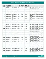
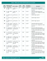
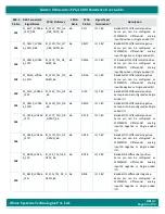
190
PL_AM14_LVDS
67_L24N
IO_L24N_T3U_
N11_67
67
AM14
IO, 1.8V
Bank67 IO24 differential negative.
Same pin can be configured as Single
ended I/O.
192
PL_AL14_LVDS6
7_L24P
IO_L24P_T3U_
N10_67
67
AL14
IO, 1.8V
Bank67 IO24 differential positive.
Same pin can be configured as Single
ended I/O.
194
PL_AT13_T3U_N
12_67
IO_T3U_N12_6
7
67
AT13
IO, 1.8V
Bank67 Single ended I/O.
196
PL_AT14_T2U_N
12_67
IO_T2U_N12_6
7
67
AT14
IO, 1.8V
Bank67 Single ended I/O.
198
PL_BB16_T1U_N
12_67
IO_T1U_N12_6
7
67
BB16
IO, 1.8V
Bank67 Single ended I/O.
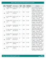
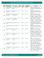
170
PL_AN27_LVDS6
5_L23N_PERSTN
1_SDA
IO_L23N_T3U_
N9_PERSTN1_I2
C_SDA_65
65
AN27
IO, 1.8V
Bank65 IO23 differential negative.
Same pin can be configured as Single
ended I/O.
116
PL_AV28_LVDS6
5_L14N_A05_D2
1_GC
IO_L14N_T2L_N
3_GC_A05_D21
_65
65
AV28
IO, 1.8V
Bank65 IO14 differential negative.
Same pin can be configured as GC Global
Clock Input differential positive or Single
ended I/O.
118
PL_AV27_LVDS6
5_L14P_A04_D2
0_GC
IO_L14P_T2L_N
2_GC_A04_D20
_65
65
AV27
IO, 1.8V
Bank65 IO14 differential positive.
Same pin can be configured as GC Global
Clock Input differential positive or Single
ended I/O.
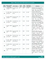
126
PL_AW26_LVDS
65_L13N_A07_D
23_GC
IO_L13N_T2L_N
1_GC_QBC_A07
_D23_65
65
AW26
IO, 1.8V
Bank65 IO13 differential negative.
Same pin can be configured as GC Global
Clock Input differential positive or Single
ended I/O.
124
PL_AV26_LVDS6
5_L13P_A06_D2
2_GC
IO_L13P_T2L_N
0_GC_QBC_A06
_D22_65
65
AV26
IO, 1.8V
Bank65 IO13 differential positive.
Same pin can be configured as GC Global
Clock Input differential positive or Single
ended I/O.
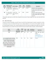
132
PL_AY28_LVDS6
5_L12N_A09_D2
5_GC
IO_L12N_T1U_
N11_GC_A09_D
25_65
65
AY28
IO, 1.8V
Bank65 IO12 differential negative.
Same pin can be configured as GC Global
Clock Input differential positive or Single
ended I/O.
130
PL_AW28_LVDS
65_L12P_A08_D
24_GC
IO_L12P_T1U_
N10_GC_A08_D
24_65
65
AW28
IO, 1.8V
Bank65 IO12 differential positive.
Same pin can be configured as GC Global
Clock Input differential positive or Single
ended I/O.

