REL0.1
Page 59 of 95
Kintex Ult FPGA SOM Hardware User Guide
iWave Systems Technologies Pvt. Ltd.
B2B-2
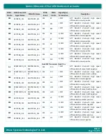
Pin No
B2B Connector2
Signal Name
FPGA Pin Name
FPGA
Bank
FPGA
Pin No
Signal Type/
Termination*
Description
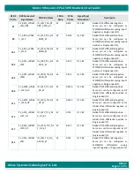
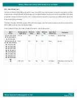
88
PL_BC14_LVDS67
_L6P
IO_L6P_T0U_N10
_AD6P_67
67
BC14
IO, 1.8V
Bank67 IO6 differential positive.
Same pin can be configured as
PLSYSMON differential analog input6
positive or Single ended I/O.
90
PL_BC13_LVDS67
_L6N
IO_L6N_T0U_N11
_AD6N_67
67
BC13
IO, 1.8V
Bank67 IO6 differential negative.
Same pin can be configured as
PLSYSMON differential analog input6
negative or Single ended I/O.
92
PL_AU13_LVDS6
7_L15P
IO_L15P_T2L_N4
_AD11P_67
67
AU13
IO, 1.8V
Bank67 IO15 differential positive.
Same pin can be configured as
PLSYSMON
differential
analog
input11 positive or Single ended I/O.
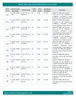
94
PL_AV13_LVDS67
_L15N
IO_L15N_T2L_N5
_AD11N_67
67
AV13
IO, 1.8V
PL Bank67 IO15 differential negative.
Same pin can be configured as
PLSYSMON
differential
analog
input11 negative or Single ended I/O.
96
PL_AV14_LVDS67
_L16N_QBC
IO_L16N_T2U_N7
_QBC_AD3N_67
67
AV14
IO, 1.8V
Bank67 IO16 differential negative.
Same pin can be configured as
PLSYSMON differential analog input3
negative or Single ended I/O.
98
PL_AU14_LVDS6
7_L16P_QBC
IO_L16P_T2U_N6
_QBC_AD3P_67
67
AU14
IO, 1.8V
Bank67 IO16 differential positive.
Same pin can be configured as
PLSYSMON differential analog input3
positive or Single ended I/O.
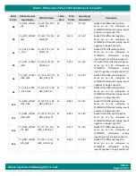
100
PL_BB15_LVDS67
_L10P_QBC
IO_L10P_T1U_N6
_QBC_AD4P_67
67
BB15
IO, 1.8V
Bank67 IO10 differential positive.
Same pin can be configured as
PLSYSMON differential analog input4
positive or Single ended I/O.
102
PL_BB14_LVDS67
_L10N_QBC
IO_L10N_T1U_N7
_QBC_AD4N_67
67
BB14
IO, 1.8V
Bank67 IO10 differential negative.
Same pin can be configured as
PLSYSMON differential analog input4
negative or Single ended I/O.
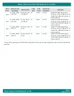
104
PL_BA12_LVDS67
_L7P_QBC
IO_L7P_T1L_N0_
QBC_AD13P_67
67
BA12
IO, 1.8V
Bank67 IO7 differential positive.
Same pin can be configured as
PLSYSMON
differential
analog
input13 positive or Single ended I/O.
106
PL_BB12_LVDS67
_L7N_QBC
IO_L7N_T1L_N1_
QBC_AD13N_67
67
BB12
IO, 1.8V
Bank67 IO7 differential negative.
Same pin can be configured as
PLSYSMON
differential
analog
input13 negative or Single ended I/O.

