REL0.1
Page 47 of 95
Kintex Ult FPGA SOM Hardware User Guide
iWave Systems Technologies Pvt. Ltd.
2.8.1.4
Data UART Interface
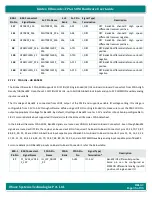
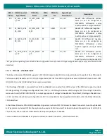
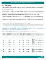
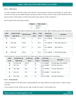
The Kintex Ult FPGA SOM supports two DATA UART interface on Board-to-Board Connector2. The pins from eSDHC
controller of alternate function are used in the Data UART interface. This controller supports full-duplex asynchronous receiver and
transmitter path with autobaud rates.
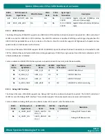
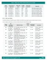
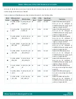
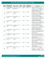
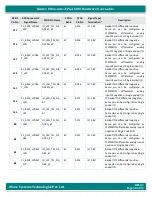
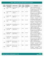
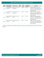
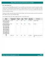
For more details on Data UART pinouts on Board-to-Board Connector2, refer the below table.
B2B-2
Pin No
B2B Connector2
Signal Name
LS1021A Pin Name
LS1021A
Pin No
Signal Type/
Termination
Description
50
LS_LPUART3_SOUT SDHC_CMD/GPIO2_0
4/LPUART3_SOUT
E2
O
Data UART Transmit Data
52
LS_LPUART3_SIN
SDHC_DAT0/GPIO2_
05/LPUART3_SIN
E1
I
Data UART Receive Data
81
LS_LPUART5_SOUT SDHC_DAT1/GPIO2_
06/LPUART2_RTS_B/
LPUART5_SOUT
F2
O
Data UART Transmit Data
79
LS_LPUART5_SIN
SDHC_DAT2/GPIO2_
07/LPUART2_CTS_B/
LPUART5_SIN
F1
I
Data UART Receive Data
2.8.1.5
I2C Interface
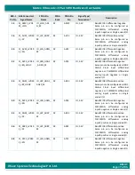
The Kintex Ult FPGA SOM supports two I2C interface on Board-to-Board Connector2. The I2C controller of LS1021A
processor’s
is used for I2C interface with the standard NXP I2C bus protocol. It can function as a master or a slave in a multi-master
design. Since flexible I2C standard allows multiple devices to be connected to the single bus, I2C2 interface is also connected to On-
SOM PMIC with I2C address 0x58 in the Kintex Ult FPGA SOM. Also, one more I2C interface (I2C1) can be taken out on
Board-to-Board Connector2.
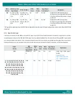
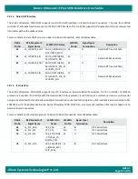
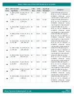
For more details on I2C Interface pinouts on Board-to-Board Connector2, refer the below table.
B2B-2
Pin No
B2B Connector2
Signal Name
LS1021A Pin
Name
LS1021A
Pin No
Signal Type/
Termination
Description
46
LS_IIC1_SDA
IIC1_SDA
P6
IO
I2C1 Serial Data
48
LS_IIC1_SCL
IIC1_SCL
N6
O
I2C1 Serial Clock
76
LS_IIC2_SCL
IIC2_SCL/GPIO4
_27/SDHC_CD_
B/SPI2_PCS3
K1
O
I2C2 Serial Clock
78
LS_IIC2_SDA
IIC2_SDA/GPIO4
_28/SDHC_WP/
SPI2_PCS4
L1
IO
I2C2 Serial Data

