ADwin-Pro II
Hardware, manual Dec. 2018
79
Pro II: Analog Input Modules
Pro II-AIn-F-4/16 Rev. E
ADwin
Look out: While a block is read, other processes even with higher priority
may be delayed. The probability of a delay rises with the block size.
– The time offset between continuous conversion and blockwise reading
demands a data buffer. Therefore, the initialization of the burst
sequence must allocate sufficient memory range (
P2_Burst_Init
,
parameter
samples
).
Event Inputs
With module version Pro II-AIn-F-4/16-D Rev. E (D-Sub female connector), a
burst sequence can be controlled by external event signals, i.e. each (result-
ing) event signal has a measurement value stored.
As an option one channel of the burst sequence may be used as time channel,
which holds the counter value of the internal module timer for each event sig-
nal.
The module is equipped with 3 differential event inputs:
EVENT/A
,
B
,
ENABLE
,
whose signals are processed to the resulting event signal. This pre-processing
of signals be configured with
P2_Event2_Config
.
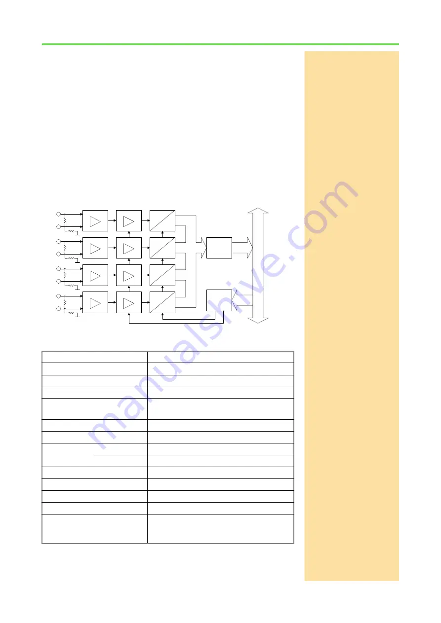
Fig. 61 – Pro II-AIn-F-4/16 Rev. E: Block diagram
Input channels
4 differential
Resolution
16 Bit
Conversion time
0.25µs (per ADC)
Input band width
0 … 600kHz
Memory size (since rev. E04)
256MiB or
2
27
= 134217728 values total
Measurement range
±10V with max. offset 3.5 V
Gain
1, 2, 4, 8 software selectable
Accuracy
INL
typical ±1.2 LSB, max. ±5 LSB
DNL
typical ±0.5 LSB, max. ±1 LSB
Input resistance
330k
Ω,
±2%
Input over-voltage
±20V
Offset error
adjustable
Offset drift
±30ppm/ºC of full scale range
Event input (D-Sub only)
3 differential;
RS422/485 compatible (5 V differential,
120
Ω
bus terminating resistor)
Fig. 62 – Pro II-AIn-F-4/16 Rev. E: Specification
ADwin-Pr
o
bu
s
A
D
1
2
4
addr.
data
Data
Register
InAmp
+
-
A
D
InAmp
+
-
A
D
InAmp
+
-
A
D
InAmp
+
-
3
data
+
–
330k
330k
+
–
330k
330k
+
–
330k
330k
+
–
330k
330k
Address
Decoder
PGA
Vu= 1, 2, 4, 8
PGA
Vu= 1, 2, 4, 8
PGA
Vu= 1, 2, 4, 8
PGA
Vu= 1, 2, 4, 8


