background image

ADwin-Pro II

 Hardware, manual Dec. 2018

53

Pro II: Analog Input Modules

Pro II-AIn-8/18 Rev. E

ADwin

5.5.1 Pro II-AIn-8/18 Rev. E

Analog input module Pro II-AIn-8/18 Rev. E with an 18-bit ADC, 8 differential
inputs and a programmable amplifier (PGA). The module can be combined
with amplifiers, Pro-TC and Pro-PT modules.

The module can be ordered in the following variants:

TiCo processor

The variants Pro II-AIn-8/18-xxx-TiCo additionally provide a freely programma-
ble 

TiCo

 processor with 28 KiByte data memory and 28 KiByte program

memory, which has access to all inputs of the module. Find more information
about use and programming of the 

TiCo

 processor in the manual 

TiCoBasic

.

If you store a 

TiCoBasic

 program in the 

TiCo

 bootloader, the program is auto-

matically loaded into the 

TiCo

 processor and started on power-up. Thus, the

module can run on its own and independently from the CPU module of the

ADwin-Pro II

 system.

low pass filter

The variants Pro II-AIn-8/18-xxx-LP contain an input filter, a 4th grade low pass
of Butterworth type. According to the variant the frequency is set to 5kHz,
10kHz, or 50kHz.

The inputs are available with shielded LEMO connectors (1-pole, CAMAC
European norm) or a DSub socket 37-pin, see fig. 36.

The module Pro II-AIn-8/18 Rev. E has an input voltage range of ±10V and a
software selectable gain of 1, 2, 4 or 8. The adjustment of gain and offset is
done by software (see chapter 6 "Calibration").

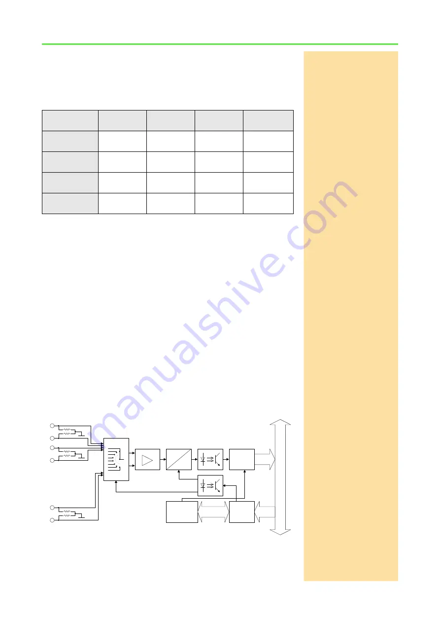
The module includes a sequential control, which can read measurement val-
ues from several or all input channels sequentially.

The module can control an upper and lower limit for each channel separately.

Fig. 34 – Pro II-AIn-8/18 Rev. E: Block diagram

no filter

filter 5kHz

filter 50kHz

filter 10kHz, 

range ±30V

LEMO 1-pole

AIn-8/18

AIn-8/18-

LP5

AIn-8/18-

LP-30V

LEMO 1-pole,
TiCo processor

AIn-8/18-

LP50-TiCo

AIn-8/18-

LP-30V-TiCo

D-Sub

AIn-8/18-D

AIn-8/18-

LP5-D

AIn-8/18-

LP-30V-D

D-Sub,
TiCo processor

AIn-8/18-

LP50-D-TiCo

AIn-8/18-LP-

30V-D-TiCo

ADwin-Pro

II

bus

A

D

1

2

8

.....

addr.

data

Data

Registers

Address

Decoder

MUX

InAmp

+

-

.....

Sequence

Control

control

+

-

100k
100k

+

-

100k
100k

+

-

100k
100k

Summary of Contents for ADwin-Pro II

Page 1: ...ADwin Pro II System and hardware description ADwin Pro II Hardware manual Dec 2018...

Page 2: ...Dec 2018 For any questions please don t hesitate to contact us Hotline 49 6251 96320 Fax 49 6251 5 68 19 E Mail info ADwin de Internet www ADwin de J ger Com putergesteuerte Messtechnik GmbH Rheinstra...

Page 3: ...Pro I modules 11 5 2 Setting the module s addresses Pro I modules too 11 5 3 Processor modules 13 5 4 Pro II Multi IO Modules 23 5 5 Pro II Analog Input Modules 52 5 6 Pro II Analog Output Modules 92...

Page 4: ...tion Information refers to further information in this documentation or to other sources such as manuals data sheets literature etc C ADwin File names and paths are placed in angle brackets and charac...

Page 5: ...eet the various requirements for measurement and control tasks the system can be equipped with the following modules analog input modules and analog output modules digital input modules and digital ou...

Page 6: ...this documentation and in other mentioned manuals Qualified personnel Programming start up and operation as well as the modification of program parameters must be performed only by appropriately qual...

Page 7: ...a the enclosure by using screen clips Supply voltage Operate the device with the defined and fitting supply voltage For operation with an external power supply the instructions of the manufacturer app...

Page 8: ...and one lower bearing Pay attention to the color of the bearings There are different offset bearings for Pro I and Pro II modules White bearings Pro II modules Black bearings Pro II modules The proce...

Page 9: ...recognize the right position easily by the color of the bearings White bearings Modules for Pro II bus Black bearings Modules for Pro I bus Output modules Pro AOut x with Rev A may not be used for te...

Page 10: ...the system Fig 3 Enclosure ADwin Pro II DC Detailed view of the pin assignment At the rear of the enclosure above the power supply connector you will find a label with the revision number Number of S...

Page 11: ...y cable rear of the enclosure At the rear of the enclosure above the power supply connector you will find a label with the revision number Number of Slots 16 Main dimensions l x w x h Slot area w x h...

Page 12: ...Enclosure ADwin Pro II light Number of Slots 7 Main dimensions l x w x h Slot area w x h 336mm 234mm 146mm incl feet 42 HP 3 U Power supply unit 100 240V AC at 50 60Hz switching mode power supply uppe...

Page 13: ...h the revision number The enclosure is delivered with a power supply female connector The plug may be ordered as follows Number of Slots 7 Main dimensions l x w x h Slot area w x h 336mm 234mm 146mm i...

Page 14: ...e enclosure you will find a label with the revision number Number of Slots 5 Main dimensions l x w x h Slot area w x h 253mm 147 3mm 146mm incl feet 20 HP 3 U External power supply unit external power...

Page 15: ...ts module group Each module is member of a module group Pro I modules functional group CPU processor modules Pro I modules functional group ADC analog input modules Pro I modules functional group DAC...

Page 16: ...ddress A fieldbus module uses 32 addresses group EXT the address alloca tion is shown in fig 13 Module no Settings of DIP switches 1 2 3 4 5 6 7 8 1 1 0 0 0 0 0 0 0 2 0 1 0 0 0 0 0 0 3 1 1 0 0 0 0 0 0...

Page 17: ...nection Communication with other ADwin Pro modules via internal Pro bus Communication with possibly existing TiCo processors on Pro II modu les via internal Pro bus Start and run the user defined proc...

Page 18: ...o program memory PM data memory DM and free for use extra memory EM Each memory section has a size of 256 KiB Fig 15 Pro CPU T11 ENET Front panel The processor module show the mode of operation by LED...

Page 19: ...ADwinPro_All inc to be included In parallel all other include files for Pro modules should be deleted from the program PROCESSDELAY The time unit of the Processdelay cycle time is 3 3 ns for both high...

Page 20: ...l processing1 of both instruction groups and obtains a much faster processing of AD basic processes This also means that the instruction groups are main ly processed independently in respect to timing...

Page 21: ...ude file ADwinPro_All inc contains the following instructions Suitable for casing Pro II Processor XILINX ZYNQ with Dual Core ARM Cortex A9 Clock rate 1000MHz Calculation resolution for float values 6...

Page 22: ...elay corresponds to 2 1 s a greater cycle time can be achieved using an auxiliary variable READ_TIMER The time unit of 1 ns is also true for the internal counter i e counter que ries with Read_Timer m...

Page 23: ...device If the storage device is built with an open board stick the delivered pla stic sheet to the open board Without sheet the board can get into con tact with the casing and generate errors An instr...

Page 24: ...ule can format read and write storage devices with EXT3 or FAT32 file system The EXT3 file system is case sensitive FAT32 is not Please note that ADbasic can read only files with a size of up 2 GiB Us...

Page 25: ...inc contains the following instructions Function Instruction Set up the storage device Storage_Create_Partitions_xxx Storage_Format_xxx Mount the file system Storage_Mount_xxx Storage_Unmount_xxx File...

Page 26: ...ications Programming in ADbasic The watchdog reset signal sets the digital and analog outputs at Pro modules to those values which correspond to the configuration after power up nor mally digital 0 or...

Page 27: ...n 5V TTL 31 Analog input 16 s e 8 diff 1 ADC 18 bit 10V Max conversion time 2 s max sample 500 ksample s Analog output 4 4 DAC 16 Bit 10V Settling time 9 s Transistor output 4 5 30 VDC external 200mA...

Page 28: ...see fig 17 The inputs are connected via a multiplexer to the ADC The ADC has a reso lution of 18 bit and can run with a sampling rate of up to 500kSamples s Analog inputs single ended Analog outputs d...

Page 29: ...of the DACs is set to 10V bipolar and can t be changed Offset and gain are adjusted by software see chapter 6 Calibra tion The outputs are available on a 37 pin D Sub female connector for pin assign m...

Page 30: ...ry serves as data and program memory You prgram the TiCo processor with TiCoBasic The TiCo processor has access to all analog and digital input and output chan nels as does the ADwin CPU Find more inf...

Page 31: ...s to 0 01 FSR Output voltage 10V Output current max 5mA per channel for optimal function Accuracy INL 2 LSB typical Accuracy DNL 1 LSB typical Offset error adjustable Gain error adjustable Digital In...

Page 32: ...ersion P2_Read_ADC_SConv P2_Read_ADC_SConv24 Use sequence control P2_Seq_Init P2_Seq_Start P2_Seq_Read P2_Seq_Read24 P2_SEQ_Read_Packed P2_Seq_Wait Control input limits P2_ADC_Read_Limit P2_ADC_Set_Li...

Page 33: ...ad_ADC24 Read value and start new con version Read_ADC_SConv Read_ADC_SConv24 Use sequence control Seq_Init Seq_Start Seq_Read Seq_Read24 Seq_Wait Control input limits ADC_Read_Limit ADC_Set_Limit Ana...

Page 34: ...r P2_TiCo_Reset P2_TiCo_Start P2_TiCo_Stop P2_Get_TiCo_Bootloader_ Status P2_Get_TiCo_Status P2_Workload Control TiCo processes P2_Process_Status P2_TiCo_Get_Processdelay P2_TiCo_Set_Processdelay P2_T...

Page 35: ...1 differential Connector Conn2 Fig 22 Pro II MIO 4 ET1 Rev E Pin assignment MIO 4 ET1 IN OUT L A RUN L A ERR EtherCAT Comm 1 Comm 2 ANALOG IN 9 ANALOG IN 10 ANALOG IN 11 ANALOG IN 12 ANALOG IN 13 ANAL...

Page 36: ...ution of 18 bit and can run with a sampling rate of up to 500kSamples s The module has an input voltage range of 10V and a software selectable gain of 1 2 4 or 8 The adjustment of gain and offset is d...

Page 37: ...nput EVENT a signal can trigger a process which will be pro cessed at once and completely see ADbasic manual The digital channels are available on a 37 pin D Sub female connector for pin assignment se...

Page 38: ...inputs are provided on the 25 pole D Sub connector Conn2 pin assign ment see fig 22 Fig 27 Pro II MIO 4 ET1 Rev E Block diagram optocouple inputs SSI Decoder An incremental encoder with SSI interface...

Page 39: ...ess the frequency of the measure ment can be determined by getting the difference of two read latch val ues because this difference defines the number of pulses between the two reading processes Four...

Page 40: ...cover page of the manual The EtherCAT slave can only be accessed from TiCoBasic You initialize slave using the instruction MIO_ECAT_Init Afterwards you project the EtherCAT bus with a configuration to...

Page 41: ...s Input channels 16 single ended 8 differential via multiplexer Resolution 18 Bit Conversion time max 2 s Sampling rate max 500ksps Multiplexer settling time 5 s Measurement range 10V Gain 1 2 4 8 sel...

Page 42: ...jumpers 0 5V 0 12V 0 24V Switching threshold for 0 low 0 0 8V 0 1 6V 0 3 2V Switching threshold for 1 high 4 5 5V 10 12V 20 24V Input over voltage 5V 8V 5V 16V 5V 30V Switching time 100ns Isolation 42...

Page 43: ...tion Range Instructions Analog Inputs Set inputs to single ended or differential P2_SE_Diff Do a single conversion com plete or step by step P2_ADC P2_ADC24 P2_Set_Mux P2_Start_Conv P2_Wait_EOC P2_Rea...

Page 44: ...2_Cnt_Get_Status P2_Cnt_Latch P2_Cnt_Sync_Latch P2_Cnt_Read P2_Cnt_Read4 P2_Cnt_Read_Latch P2_Cnt_Read_Latch4 Use PWM counter P2_Cnt_PW_Enable P2_Cnt_PW_Latch P2_Cnt_Get_PW P2_Cnt_Get_PW_HL P2_Cnt_Rea...

Page 45: ...set output signals MIO_Digout MIO_Digout_Long MIO_Get_Digout_Long Use latch register MIO_Dig_Latch MIO_Dig_Write_Latch Optocouple Inputs Query input signals MIO_Digin_Long Use latch register MIO_Dig_L...

Page 46: ...Pro II Multi IO Modules Pro II MIO 4 ET1 Rev E ADwin 42 ADwin Pro II Hardware manual Dec 2018 Use interrupt and event inputs Event_Enable Event_Read Event_Config Trigger_Event Range Instructions...

Page 47: ...Data exchange with the TiCo processor via global variables P2_TDrv_Init P2_GetData_Long P2_Get_Par P2_Get_Par_Block P2_SetData_Long P2_Set_Par P2_Set_Par_Block P2_Get_TiCo_RingBuffer P2_Set_TiCo_RingB...

Page 48: ...ons are described in the following sections Transistor Outputs TRA Optocouple Inputs OPT SSI decoder Counter block TiCo processor Technical Specification Programmierung with ADbasic and TiCoBasic Tran...

Page 49: ...evel output on TRA outputs Optocouple Inputs The module Pro II MIO D12 Rev E provides 12 channels of optically isolated digital inputs The input voltage range can be set by jumpers 5V 12V 24V The swit...

Page 50: ...ve RS422 485 levels You can set the clock rate 6kHz 12 5MHz as well as the data resolution up to 32 bit of the decoder via software Pin assignment of the decoder inputs see fig 30 The input SSI IN can...

Page 51: ...fference defines the number of pulses between the two reading pro cesses Four edge evaluation A and B signals The four edge evaluation changes the signals which should be 90 pha se shifted of a connec...

Page 52: ...hing voltage VCC 5 30V DC durch externe Spannungsversorgung Switching current 200mA max per channel Voltage drop 0 5V Switching time 2 5 s Isolation 42V channel channel channel GND common ground for a...

Page 53: ...Sub female connector Fig 33 Pro II MIO D12 Rev E Specification Range Instructions Transistor Outputs Set and reset output signals P2_MIO_Digout P2_MIO_Digout_Long P2_MIO_Get_Digout_Long Use latch regi...

Page 54: ...atus General Use LED P2_Check_LED P2_Set_LED Synchronize P2_Sync_All P2_Sync_Enable P2_Sync_Stat Use interrupt and event inputs P2_Event_Enable P2_Event_Read P2_Event_Config Range Instructions Range I...

Page 55: ...ent_Config Trigger_Event Range Instructions Function Instructions Data exchange with the TiCo processor via global variables P2_TDrv_Init P2_GetData_Long P2_Get_Par P2_Get_Par_Block P2_SetData_Long P2...

Page 56: ...8 18 AIn 8 18 TiCo AIn 32 18 D AIn 32 18 D TiCo AIn 16 18 C AIn 8 18 8B AIn 16 18 8B Revision E E E E E E E Number ADC 1 1 1 1 1 1 1 Resolution Bit 18 18 18 18 18 18 18 Max conv time s 2 2 2 2 2 2 2 m...

Page 57: ...ts Pro II AIn 8 18 xxx LP contain an input filter a 4th grade low pass of Butterworth type According to the variant the frequency is set to 5kHz 10kHz or 50kHz The inputs are available with shielded L...

Page 58: ...rift 30ppm C TiCo processor only with Pro II AIn 8 18 L2 TiCo Rev E Processor type TiCo1 Clock frequency 50MHz Memory size 28KiB PM internal 28KiB DM internal Connector 8 LEMO female connectors 1 pole...

Page 59: ...Do a single conversion com plete or step by step P2_ADC P2_ADC24 P2_Set_Mux P2_Start_Conv P2_Wait_EOC P2_Read_ADC P2_Read_ADC24 Read value and start new con version P2_Read_ADC_SConv P2_Read_ADC_SCon...

Page 60: ...essor P2_TiCo_Reset P2_TiCo_Start P2_TiCo_Stop P2_Get_TiCo_Bootloader_ Status P2_Get_TiCo_Status P2_Workload Control TiCo processes P2_Process_Status P2_TiCo_Get_Processdelay P2_TiCo_Set_Processdelay...

Page 61: ...module is set to 16 differential inputs The module Pro II AIn 32 18 D Rev E has an input voltage range of 10V and a software selectable gain of 1 2 4 or 8 The adjustment of gain and offset is done by...

Page 62: ...Analoger Eingang 31 Analoger Eingang 32 AGND EVENT Analoger Eingang 1 Analoger Eingang 2 Analoger Eingang 3 Analoger Eingang 4 Analoger Eingang 5 Analoger Eingang 6 Analoger Eingang 7 Analoger Eingang...

Page 63: ...ion P2_Read_ADC_SConv P2_Read_ADC_SConv24 Use sequence control P2_Seq_Init P2_Seq_Start P2_Seq_Read P2_Seq_Read24 P2_Seq_Read24_Packed P2_Seq_Wait Control input limits P2_ADC_Read_Limit P2_ADC_Set_Lim...

Page 64: ...a single conversion com plete or step by step ADC ADC24 Set_Mux Start_Conv Wait_EOC Read_ADC Read_ADC24 Read value and start new con version Read_ADC_SConv Read_ADC_SConv24 Use LED Check_LED Set_LED...

Page 65: ...connected to one of the AGND pins The ground connection to the Pro device should be split up by switching the DIL switch see fig 42 to position GND LIFT Do not run the module without ground connectio...

Page 66: ...ENT IN 15 CURRENT IN 16 AGND EVENT CURRENT IN 1 CURRENT IN 2 CURRENT IN 3 CURRENT IN 4 CURRENT IN 5 CURRENT IN 6 CURRENT IN 7 CURRENT IN 8 CURRENT IN 9 CURRENT IN 10 CURRENT IN 11 CURRENT IN 12 CURREN...

Page 67: ...ules Pro II AIn 16 18 C Rev E ADwin Control input limits P2_ADC_Read_Limit P2_ADC_Set_Limit Synchronize P2_Sync_All Use LED P2_Check_LED P2_Set_LED Use interrupt and event inputs P2_Event_Enable P2_Ev...

Page 68: ...ound of the Pro device Alterna tively a GND level signal common for all inputs can be connected to one of the AGND pins The ground connection to the Pro device should be split up by switching the DIL...

Page 69: ...ang 16 AGND reserviert Analoger Eingang 9 Analoger Eingang 10 Analoger Eingang 11 Analoger Eingang 12 Analoger Eingang 13 Analoger Eingang 14 Analoger Eingang 15 Analoger Eingang 16 AGND reserviert AG...

Page 70: ...nalog Input Modules Pro II AIn 8 18 8B Rev E ADwin 66 ADwin Pro II Hardware manual Dec 2018 Use interrupt and event inputs P2_Event_Enable P2_Event_Read P2_Event_Config P2_Event2_Config Function Instr...

Page 71: ...evice Alterna tively a GND level signal common for all inputs can be connected to one of the AGND pins The ground connection to the Pro device should be split up by switching the DIL switch see fig 42...

Page 72: ...14 Excitation 15 Sensor 15 Excitation 16 Sensor 16 1 2 3 4 5 6 7 8 9 10 11 12 13 14 15 16 17 18 19 20 21 22 23 24 25 26 27 28 29 30 31 32 33 34 35 36 37 reserviert reserviert 19AD1002 DC DC CONVERTER...

Page 73: ...8 69 Pro II Analog Input Modules Pro II AIn 16 18 8B Rev E ADwin Synchronize P2_Sync_All Use LED P2_Check_LED P2_Set_LED Use interrupt and event inputs P2_Event_Enable P2_Event_Read P2_Event_Config P2...

Page 74: ...ontinuously does single measurements until the sequence is stopped The data is stored in a fifo like memory As an option the module can return the moving average of 2 32 measure ment values instead of...

Page 75: ...nput band width 0 4MHz Memory size 256MiB or 227 134217728 values total Measurement range 10V with max offset 3 5 V Accuracy INL typical 1 2 LSB max 5 LSB DNL typical 0 5 LSB max 1 LSB Input resistanc...

Page 76: ...s 00 Multi Contact type EGG BNC connector AIN AIN 1 pole LEMO connector D Sub connector ANALOG IN 1 ANALOG IN 2 ANALOG IN 3 ANALOG IN 4 ENABLE B AGND EVENT A ANALOG IN 1 ANALOG IN 2 ANALOG IN 3 ANALOG...

Page 77: ...urst_Read P2_Burst_Read_Index P2_Burst_Read_Index P2_Burst_Read_Unpacked1 2 4 P2_Burst_CRead_Unpacked1 2 4 P2_Burst_CRead_Pos_Unpacked1 2 4 Synchronize P2_Sync_All P2_Sync_Enable P2_Sync_Stat Control...

Page 78: ...e that is a defined number of single measure ments Continuous burst sequence The ADbasic program starts a burst mea surement sequence that continuously does single measurements until the sequence is s...

Page 79: ...s 8 differential Resolution 14 Bit Conversion time 0 02 s per ADC Sampling rate 4 50000ksps per ADC or 8 25000ksps per ADC Input band width 0 4MHz Memory size 256MiB or 227 134217728 values total Meas...

Page 80: ...ANALOG IN 6 ANALOG IN 7 ANALOG IN 8 ENABLE diff RS422 B diff RS422 AGND EVENT A diff RS422 ANALOG IN 1 ANALOG IN 2 ANALOG IN 3 ANALOG IN 4 ANALOG IN 5 ANALOG IN 6 ANALOG IN 7 ANALOG IN 8 ENABLE diff R...

Page 81: ...2_Burst_Read_Index P2_Burst_Read_Unpacked1 2 4 8 P2_Burst_CRead_Unpacked1 2 4 8 P2_Burst_CRead_Pos_Unpacked1 2 4 8 Synchronize P2_Sync_All P2_Sync_Enable P2_Sync_Mode P2_Sync_Stat Control input limits...

Page 82: ...ingle measurements until the sequence is stopped The data is stored in a fifo like memory As an alternative to the operation modes above the module can perform a simultaneous conversion on all channel...

Page 83: ...odule is equipped with 3 differential event inputs EVENT A B ENABLE whose signals are processed to the resulting event signal This pre processing of signals be configured with P2_Event2_Config Fig 61...

Page 84: ...onnectors Fig 62 Pro II AIn F 4 16 Rev E Specification AIN AIN PE AIN AIN 2 pole LEMO female connector series 00 Multi Contact type EGG BNC connector AIN AIN 1 pole LEMO connector D Sub connector ANAL...

Page 85: ..._Burst_Status P2_Burst_Reset P2_Burst_Read P2_Burst_Read_Index P2_Burst_Read_Index P2_Burst_Read_Unpacked1 2 4 P2_Burst_CRead_Unpacked1 2 4 P2_Burst_CRead_Pos_Unpacked1 2 4 Synchronize P2_Sync_All P2_...

Page 86: ...ea surement sequence that continuously does single measurements until the sequence is stopped The data is stored in a fifo like memory As an alternative to the operation modes above the module can per...

Page 87: ...olled by external event signals i e each result ing event signal has a measurement value stored As an option one channel of a burst sequence may be used as time channel holding the counter value of th...

Page 88: ...emale connectors Module width 5 HP with BNC connectors 10 HP Fig 66 Pro II AIn F 8 16 Rev E Specification AIN AIN PE AIN AIN 2 pole LEMO female connector series 00 Multi Contact type EGG BNC connector...

Page 89: ...version P2_Burst_Init P2_Burst_Start P2_Burst_Stop P2_Burst_Status P2_Burst_Reset P2_Burst_Read P2_Burst_Read_Index P2_Burst_Read_Index P2_Burst_Read_Unpacked1 2 4 8 P2_Burst_CRead_Unpacked1 2 4 8 P2_...

Page 90: ...sequence control This disburdens compared to single measurements with the instruction P2_ADCF the processor module which only reads and proces ses the converted measurement values The conversion can...

Page 91: ...ge Connector 4 LEMO female connectors 1 pole or 4 LEMO female connectors 2 pole or 37 pin D Sub female connector or 4 BNC connectors Fig 71 Pro II AIn F 4 18 Rev E Specification ANALOG IN 1 ANALOG IN...

Page 92: ...re sequence control P2_ADCF_Mode Do a single conversion com plete or step by step P2_ADCF P2_ADCF24 P2_Start_ConvF P2_Wait_EOCF P2_Read_ADCF P2_Read_ADCF24 Read several values P2_Read_ADCF32 P2_Read_A...

Page 93: ...sequence control This disburdens compared to single measurements with the instruction P2_ADCF the processor module which only reads and proces ses the converted measurement values The conversion can...

Page 94: ...37 pin D Sub female connector or 8 BNC connectors Module width 5 HP with BNC connectors 10 HP Fig 76 Pro II AIn F 8 18 Rev E Specification ANALOG IN 1 ANALOG IN 2 ANALOG IN 3 ANALOG IN 4 ANALOG IN 5...

Page 95: ...2_ADCF_Mode Do a single conversion com plete or step by step P2_ADCF P2_ADCF24 P2_Start_ConvF P2_Wait_EOCF P2_Read_ADCF P2_Read_ADCF24 Read several values P2_Read_ADCF32 P2_Read_ADCF4 P2_Read_ADCF4_24...

Page 96: ...ADwin Pro I be found in the manual ADwin Pro Hardware from page 65 Module name AOut 4 16 AOut 4 16 TiCo AOut 8 16 AOut 8 16 TiCo AOut 1 16 Revision E E E E E Number DAC 4 4 8 8 1 Resolution bit 16 16...

Page 97: ...nd programming of the TiCo processor in the manual TiCoBasic If you store a TiCoBasic program in the TiCo bootloader the program is auto matically loaded into the TiCo processor and started on power u...

Page 98: ...frequency 50MHz Memory size 28KiB PM internal 28KiB DM internal Connector 4 LEMO female connectors 1 pole or 4 LEMO female connectors 2 pole or 37 pin D Sub female connector or 4 BNC connectors Fig 80...

Page 99: ...ructions Output values P2_DAC P2_DAC4 P2_DAC4_Packed Output values step by step P2_Write_DAC P2_Write_DAC4 P2_Write_DAC4_Packed P2_Write_DAC32 P2_Start_DAC Synchronize P2_Sync_All P2_Sync_Enable P2_Sy...

Page 100: ...about use and programming of the TiCo processor in the manual TiCoBasic If you store a TiCoBasic program in the TiCo bootloader the program is auto matically loaded into the TiCo processor and started...

Page 101: ...Connector 8 LEMO female connectors 1 pole or 8 LEMO female connectors 2 pole or 37 pin D Sub female connector or 8 BNC connectors Module width 5 HP with BNC or LEMO 2 pole 10 HP Fig 84 Pro II AOut 8...

Page 102: ...acked P2_DAC8 P2_DAC8_Packed Output values step by step P2_Write_DAC P2_Write_DAC4 P2_Write_DAC4_Packed P2_Write_DAC8 P2_Write_DAC8_Packed P2_Write_DAC32 P2_Start_DAC Synchronize P2_Sync_All P2_Sync_E...

Page 103: ...tput voltage value Fig 87 Pro II AOut 1 16 Rev E Pin assignment and front cover To output DAC values there are 3 variants 1 Single value output 2 Continuous output via an output Fifo The output values...

Page 104: ...ternally triggered ADbasic process which is processed immediately and completely see ADbasic man ual TiCo processor The module provides the freely programmable TiCo processor with 28kiB pro gram memor...

Page 105: ...ssor type TiCo1 Clock rate 50MHz Memory size 28kiB PM internal 28kiB DM internal 256MiByte DRAM external Connector 37 pin D Sub female connector SMB con nector female Module width 10 HP Fig 88 Pro II...

Page 106: ...vent_Enable P2_Event_Read P2_Event_Config Function Instructions Function Instructions Analog Output Output single value DAC DAC1_DIO Output value step by step Write_DAC Start_DAC Output DAC value and...

Page 107: ...ns Data exchange with the TiCo processor via global variables P2_TDrv_Init P2_GetData_Long P2_Get_Par P2_Get_Par_Block P2_SetData_Long P2_Set_Par P2_Set_Par_Block P2_Get_TiCo_RingBuffer P2_Set_TiCo_Ri...

Page 108: ...24 DC 42 123 OPT 32 24V E Optocouple input 32 24 DC 42 126 REL 16 E Relay output 16 max 30 AC DC 500 42 128 TRA 16 E Transistor output 16 5 30 DC 200 42 130 PWM 16 E PWM output signal 16 5 TTL 132 PWM...

Page 109: ...to digital outputs as stand alone Find more on page 107 Fig 89 Pro II DIO 32 Rev E Block diagram Fig 90 Pro II DIO 32 Rev E Front panel and Pin assignment Digital inputs TTL logic Input output channel...

Page 110: ...p status All channels as inputs Connector 37 pin D Sub female connector Fig 91 Pro II DIO 32 Rev E Specification Function Instructions Configure input outputs P2_DigProg Query input signals P2_Digin_L...

Page 111: ...nels After power up all filters are disabled TiCo processor Different from variant Pro II DIO 32 Rev E the module provides in addition the freely programmable TiCo processor with 28KiB program memory...

Page 112: ...Frequency 100MHz TiCo Prozessor type TiCo1 Clock rate 50MHz Memory size 28kiB PM internal 28kiB DM internal 256MiByte DRAM external Connector 37 pin D Sub female connector Fig 94 Pro II DIO 32 TiCo R...

Page 113: ..._Clear P2_Digout_FIFO_Empty P2_Digout_FIFO_Enable P2_Digout_FIFO_Read_Timer P2_Digout_FIFO_Start P2_Digout_FIFO_Write Synchronize P2_Sync_All P2_Sync_Enable P2_Sync_Stat Use LED P2_Check_LED P2_Set_LE...

Page 114: ...ns Data exchange with the TiCo processor via global variables P2_TDrv_Init P2_GetData_Long P2_Get_Par P2_Get_Par_Block P2_SetData_Long P2_Set_Par P2_Set_Par_Block P2_Get_TiCo_RingBuffer P2_Set_TiCo_Ri...

Page 115: ...stable filter Each channel has its own filter but filter settings are the same for all channels After power up all filters are disabled TiCo processor The module provides in addition the freely progra...

Page 116: ...Prozessor type TiCo1 Clock rate 50MHz Memory size 28kiB PM internal 28kiB DM internal Connector 37 pin D Sub female connector Fig 97 Pro II DIO 32 1 TiCo Rev E Specification Function Instructions Conf...

Page 117: ...ck output sig nals P2_Digout P2_Digout_Bits P2_Digout_Long P2_Digout_Set P2_Digout_Reset P2_Get_Digout_Long Set output signals automati cally P2_Digout_FIFO_Clear P2_Digout_FIFO_Empty P2_Digout_FIFO_E...

Page 118: ...Check_LED Set_LED Setting interrupts and event input Event_Enable Trigger_Event Event_Config Function Instructions Function Instructions Data exchange with the TiCo processor via global variables P2_...

Page 119: ...t the input channels spikes can be suppressed using an adjustable filter Each channel has its own filter but filter settings are the same for all channels After power up all filters are disabled TiCo...

Page 120: ...nternal Connector 37 pin D Sub female connector Fig 101 Pro II DIO 32 TiCo2 Rev E Specification DIO 32 RB ADwin Pro bus 0 1 31 2 3 30 EVENT Data Register Data 10k 10k 10k 10k 10k 10k 10k Bus Trans cei...

Page 121: ...r edges of input chan nels P2_Digin_FIFO_Enable P2_Digin_FIFO_Read P2_Digin_Fifo_Read_Fast P2_Digin_FIFO_Read_Timer P2_Digin_FIFO_Clear P2_Digin_FIFO_Full Set spike filter P2_Digin_Filter_Init Query e...

Page 122: ...O_Read_Timer Digout_FIFO_Start Digout_FIFO_Write Use LED Check_LED Set_LED Use interrupt and event inputs Event_Enable Trigger_Event Event_Config Function Instructions Function Instructions Data excha...

Page 123: ...e TiCo2 with 128KiB program memory and 512KiB data memory The TiCo processor has access to all digital input and output channels Find more information about use and programming of the TiCo processor i...

Page 124: ...hannels as inputs Input output FIFO Size 2048 value pairs Frequency 200MHz TiCo Prozessor type TiCo2 Clock rate 100MHz Memory size 128kiB PM internal 512KiB DM internal Connector 37 pin D Sub female c...

Page 125: ...Instructions Function Instructions Configure input outputs DigProg DigProg_Bits Query input signals Digin_Long Monitor edges of input chan nels Digin_FIFO_Enable Digin_FIFO_Read Digin_FIFO_Read_Timer...

Page 126: ...essor P2_TiCo_Reset P2_TiCo_Start P2_TiCo_Stop P2_Get_TiCo_Bootloader_ Status P2_Get_TiCo_Status P2_Workload Control TiCo processes P2_Process_Status P2_TiCo_Get_Processdelay P2_TiCo_Set_Processdelay...

Page 127: ...or negative edge has occurred at the input channels Each channel is optically isolated from the system circuitry and from the other inputs The event input is optically isolated from the system as wel...

Page 128: ...ze 511 value pairs Frequency 100MHz Isolation 42V channel channel channel GND Connector 37 pin D Sub female connector Fig 107 Pro II OPT 16 Rev E Specification 19DIOCNT1003 XILINX SPARTAN XC2S150 HCPL...

Page 129: ...ADwin Pro II Hardware manual Dec 2018 125 Pro II Digital I O Modules Pro II OPT 16 Rev E ADwin Use interrupt and event inputs P2_Event_Enable P2_Event_Read P2_Event_Config Function Instructions...

Page 130: ...ve edge has occurred at the input channels Each channel is optically isolated from the system circuitry and from the other inputs The event input is optically isolated from the system as well The chan...

Page 131: ...on 0 24V Switching threshold for 0 low 0 3 2V Switching threshold for 1 high 20 24V Input over voltage 5V 30V Switching time 100ns Input FIFO Size 511 value pairs Frequency 100MHz Isolation 42V channe...

Page 132: ...ADwin Pro bus A B 0 Data EVENT 4k3 2k 560 24V 12V 5V Data Register A B 15 RELAY 0 A RELAY 1 A RELAY 2 A RELAY 3 A RELAY 4 A RELAY 5 A RELAY 6 A RELAY 7 A RELAY 8 A RELAY 9 A RELAY 10 A RELAY 11 A RELA...

Page 133: ...ional normally closed Operate time 4ms Release time 3ms Bounce time 2ms Event inputs 1 Isolation 42V channel channel chan nel GND Event input voltage 5V 12V 24V selectable via jumpers Power up status...

Page 134: ...ls as well as the event input are optically isolated from system cir cuitry Fig 115 Pro II TRA 16 Rev E Block diagram Fig 116 Pro II TRA 16 Rev E Pin assignment ADwin Pro bus Data Data Register 1k 56k...

Page 135: ...1 Isolation 42V channel channel channel GND Event input voltage 5V 12V 24V selectable via jumpers Power up status low GND external Connector 37 pin D Sub female connector Fig 118 Pro II TRA 16 Rev E S...

Page 136: ...y cycle can be still defined in 1 steps is 1000kHz above Pro II PWM 16 Rev E below Pro II PWM 16 I Rev E Fig 119 Pro II PWM 16 Rev E Block diagram Data Data A B A B NOTE Only PWM output 1 is shown for...

Page 137: ...tput current 100mA max per channel Voltage drop 0 5V max Fig 122 Pro II PWM 16 Rev E Spezifikation DGND EVENT IN PWM OUT 1 PWM OUT 2 PWM OUT 3 PWM OUT 4 PWM OUT 5 PWM OUT 6 PWM OUT 7 PWM OUT 8 PWM OUT...

Page 138: ...ions Switching time without load 3 s with load 1 2 s Event input voltage 5V 12V 24V selectable via jumpers Isolation 42 V channel channel chan nel GND Fig 122 Pro II PWM 16 Rev E Spezifikation Functio...

Page 139: ...annels is as follows The comparators run with 50MHz Edge detection The module can automatically monitor the edges of input channels signals after comparators which is performed with a frequency of 100...

Page 140: ...ndard hysteresis Comparator filter You can enable a filter which is located behind the comparators in order to suppress single spikes The number of spikes should be small com pared to the pulse width...

Page 141: ...r Bit no 31 16 15 14 2 1 0 Channel no 16 15 3 2 1 Bit no 31 24 23 22 17 16 15 0 Channel pair 15 16 13 14 3 4 1 2 Input channels 16 single ended inputs each with its own comparator Threshold adjustable...

Page 142: ...tions for the following functions Function Instructions Do mode and comparator settings P2_Comp_Init P2_Comp_Filter_Init P2_Comp_Set Query comparator bits P2_Digin_Edge P2_Digin_Long Use latch registe...

Page 143: ...power up Thus the module can run on its own and independently from the CPU module of the ADwin Pro II system Up down counter The up down counter of a block can be operated in 2 modes Clock direction...

Page 144: ...ired about PWM registers Use the evalu ation with PWM registers for special solutions only In order to evaluate PWM signals the counter values of the current and the 2 preceding counter values are sto...

Page 145: ...e set with SSI_Set_Clock from 6 1kHz 12 5MHz Resolution is set with SSI_Set_Bits up to 32 bit REM Exmaple conversion from Gray code into binary code REM Par_1 Gray value To be converted REM Par_2 Flag...

Page 146: ...has been released can start an externally triggered ADbasic process Fig 127 Pro II CNT x Rev E Front panel Fig 128 Pro II CNT I Rev E Board with jumpers CNT D COUNTER INPUT CNT I COUNTER INPUT CNT T...

Page 147: ...CLK CNTR 4 A RESERVED DGND 5V OUT 0 1A DGND 19 18 17 16 15 14 13 12 11 10 9 8 7 6 5 4 3 2 1 37 36 35 34 33 32 31 30 29 28 27 26 25 24 23 22 21 20 SSI 1 CLK CNTR 1 A CLK CNTR 1 B DIR CNTR 1 CLR LATCH...

Page 148: ...rrent typ 3 5mA max 7 5mA input voltage range selectable via jumpers 0 5V 0 12V 0 24V reliable switching threshold1 for 0 low 0 0 8V 0 1 6V 0 3 2V reliable switching threshold1 for 1 high 4 5 5V 10 12...

Page 149: ...ters Cnt_Clear Cnt_Get_Status Cnt_Latch Cnt_Sync_Latch Cnt_Read Cnt_Read_Latch Cnt_Read_Int_Register Use PWM counters Cnt_PW_Enable Cnt_PW_Latch Cnt_Get_PW_HL P2_Cnt_Read_Int_Register Use SSI decoders...

Page 150: ...Page 149 153 Module CAN 2 CAN 2 LS LIN 2 Profi SL Revision E E E E Type CAN interface with TiCo1 processor LIN bus interface Profibus interface Interface type High speed Low speed Interfaces 2 2 1 Pag...

Page 151: ...interface ARINC 429 interface with TiCo1 processor SPI master SPI slave with TiCo1 processor SPI master SPI slave with TiCo1 processor Signal type TTL differential Interfaces 2 3 2 2 Data exchange ra...

Page 152: ...LS bus Revision E E E Function FlexRay interface EtherCAT interface LS bus interface Interfaces 2 1 2 Page 190 192 217 Module SENT 4 SENT 6 SENT 4 Out Revision E E E Type SENT interface SENT interfac...

Page 153: ...ings During a measurement multiplexers connect the measuring wires with the sensor and disconnect them afterwards Then the measure ment values are available in the module so the ADwin CPU only has to...

Page 154: ...ro II Hardware manual Dec 2018 Accuracy PT100 0 05K PT500 0 1K PT1000 0 1K Ni100 0 05K Temp resolution 0 015K Drift 10ppm K I1 I2 PT100 1mA PT500 0 2mA PT1000 0 1mA Ni100 1mA Connector 37 pin D Sub fe...

Page 155: ...e D Sub connector 3 wire measurement In order to avoid the disadvantages of the 2 wire measurement the volt age drop in the measurement lines is here compensated by a second voltage source I2 To keep...

Page 156: ...o II RTD 8 Rev E Block diagram and pin assignment with 4 wire measurement LPF fg 25 kHz InAmp G 50 19 37 36 18 RT VS IEXC M1 M U X M2 EXC EXC IN RESERVED EXCITATION 1 RESERVED EXCITATION 2 RESERVED EX...

Page 157: ...e module calculates the thermo electric voltage or the temperature in Celsius or Fahrenheit from the last measurement value All calculation is based upon the norm IEC 584 1 The thermoelectric voltage...

Page 158: ...to program the module Offset drift 30ppm K of full scale range Connector Omega Subminiature Connector Type SMP Fig 138 Pro II TC 8 ISO Rev E Specifikation GND OFF GND OFF GND OFF GND OFF GND OFF GND O...

Page 159: ...l tage EX with EX 9 80V the minimum resistance is 100 with EX 1 25V it is 13 The module Pro II SG 4 18 Rev E provides the bridge excitation vol tage EX for the strain gage wiring via software the exci...

Page 160: ...each channel there are several filters F r jeden Kanal sind mehrere Filter vorhanden 1MHz at the input 2 kHz 2nd order after first amplifier 2kHz or 200 Hz 2nd order after second amplifier selectable...

Page 161: ...e acc to EX 50 400 Resolution ADC ADC conversion time 18 Bit 2 s Voltage range strain gage Voltage range analog inputs max 500mV min 15 625mV 10V Multiplexer settling time 5 s Bridge sensitivity 1 59m...

Page 162: ...cterized by so called identifiers The CAN controller supports identifiers with a length of 11 bit and 29 bit The communication that means the manage ment of bus messages is effected by 15 message obje...

Page 163: ...must be terminated with a 120 resistor only the first or the last CAN node If a termination is necessary move the DIP switch see fig 144 upward CAN nodes which are not positioned in an end location m...

Page 164: ...a message is made as follows You configure a message object to receive and define the identifier of the object instruction En_Receive The controller monitors the CAN bus if there are incoming message...

Page 165: ...er is connected to the event input of the processor The processor reacts immediately to incoming mes sages without having to control the message input polling You can enable the interrupts of several...

Page 166: ...ge objects P2_En_Receive P2_Read_Msg P2_En_Transmit P2_Transmit Set and read registers P2_Set_CAN_Reg P2_Get_CAN_Reg Use LED P2_Check_LED P2_Set_LED P2_CAN_Set_LED Use interrupt and event inputs P2_En...

Page 167: ...on and Interface Modules Pro II CAN 2 Rev E ADwin Control TiCo processes P2_Process_Status P2_TiCo_Get_Processdelay P2_TiCo_Set_Processdelay P2_TiCo_Start_Process P2_Tico_Stop_Process Transfer TiCo pr...

Page 168: ...o 64 data bytes which are characterized by so called identifiers The CAN controller supports identifiers with a length of 11 bit 12 bit and 29 bit The communication that means the management of bus me...

Page 169: ...message objects Each message object can store up to 32 messages The message objects 1 31 are built as FIFO and can either be configured to send output fifo or to receive messages input fifo In a Fifo...

Page 170: ...ontroller initialization Controlling sent messages You can define a transmit event fifo in order to control sent messages The Fifo can store the message header and an optional timestamp for each sent...

Page 171: ...of the messages because the bits 3 10 of the compared identifiers are identical 0 and the bits 0 and 1 are not compared because they are set to zero in the global mask not relevant Module revisions Di...

Page 172: ...FD_Enable_Receive_Fifo P2_CANFD_Enable_Transmit_Fifo P2_CANFD_Enable_Transmit_Queue P2_CANFD_Enable_Transmit_Event_Fifo P2_CANFD_Set_Baudrate_Nominal P2_CANFD_Set_Baudrate_Data P2_CANFD_Set_SID11 P2_C...

Page 173: ...ller CANFD_Enable_Receive_Fifo CANFD_Enable_Transmit_Fifo CANFD_Enable_Transmit_Queue CANFD_Enable_Transmit_Event_Fifo CANFD_Set_Baudrate_Nominal CANFD_Set_Baudrate_Data CANFD_Set_SID11 CANFD_Set_TDC...

Page 174: ...uctions Data exchange with the TiCo processor via global variables P2_TDrv_Init P2_GetData_Long P2_Get_Par P2_Get_Par_Block P2_SetData_Long P2_Set_Par P2_Set_Par_Block P2_Get_TiCo_RingBuffer P2_Set_Ti...

Page 175: ...mming of the TiCo processor in the TiCoBasic manual If you store a TiCoBasic program in the TiCo bootloader the program is auto matically loaded into the TiCo processor and started on power up Thus th...

Page 176: ...1 or 2 stop bits Baud rate Baud rate The physical data are between 35 Baud and 2 304 MBaud when using an RS 232 interface the maximum Baud rate is 115 2kBaud according to the specification The Baud r...

Page 177: ...TiCoBasic online help The include file RS_LIN_TiCo inc contains instructions for the following functions Programming TiCo access To access the TiCo processor from the ADwin CPU the following ADbasic i...

Page 178: ...ck P2_SetData_Long P2_Set_Par P2_Set_Par_Block P2_Get_TiCo_RingBuffer P2_Set_TiCo_RingBuffer P2_RingBuffer_Empty P2_RingBuffer_Full Control TiCo processor P2_TiCo_Reset P2_TiCo_Start P2_TiCo_Stop P2_G...

Page 179: ...odule revisions Programming TiCo processor The module provides the freely programmable TiCo processor with 28KiB pro gram memory and 28KiB data memory The TiCo processor is programmed with TiCoBasic T...

Page 180: ...possible which can be derived from an integer division of the ba sic frequency The divisor can have values between 1 0FFFFh The following table shows some common Baud rates and their divisors Fig 151...

Page 181: ..._RS P2_Set_RS Use LED P2_Check_LED P2_Set_LED P2_RS_Set_LED Function Instructions Function Instructions Initialization RS_Init RS_Reset Receiving and transmitting of data Read_Fifo Write_Fifo Check_Sh...

Page 182: ...Hardware design The connections of the LIN bus interfaces are on the 9 pin D SUB connectors the pin assignments are shown below The operating voltage range of Bat is 8V 18V For each interface there is...

Page 183: ...lave node waits until the master sends the header with the identifier which fits to the identifier of the message box Then the slave receives the data packet and stores it into the message box Module...

Page 184: ...operation status of the fieldbus node operation mode OP and interface status ST Fig 154 Pro II Profi SL Rev E Meaning of LEDs Projecting the Profibus You are projecting the Profibus with a configurat...

Page 185: ...m the master first and then the inputs If there are inputs initialized in ADbasic you have to configure outputs as correspondent in the configuration tool Number and length of data ranges must equal t...

Page 186: ...is in agreement with the European Standard EN 50170 Volume 2 This norm is provided by the Profibus user organization Profibus Nutzerorganisation e V Haid und Neu Str 7 76131 Karlsruhe Germany Phone 4...

Page 187: ...st of one or more 16 bit words command word data words or status word The 16 bits comprising each word are transmitted using Manchester code The BC controls the total data transfer of the bus using co...

Page 188: ...S1 S8 S13 which are required only for the use of the interface as bus controller or remote terminal With SMT mode all DIP switches should be set to OFF position Non suitable DIP switch settings can ca...

Page 189: ...o II Software manual The include file ADwinPro_All inc contains instructions for the following functions S8 RT1ENA OFF S13 TXINHA_1 OFF S8 RT2ENA OFF S13 TXINHA_2 OFF S7 MTSTOFF OFF S7 RAMEDC OFF S7 T...

Page 190: ...able units LRU are most commonly configured in a star or bus drop topology Each LRU may contain multiple transmitters and receivers commu nicating on different buses Data words on the bus are 32 bits...

Page 191: ...he module is comfortably programmed with ADbasic instructions The instructions are described in ADbasic online help and in the Pro II Software manual Function ARINC 429 interface with 1 transmitter 2...

Page 192: ...ceive P2_ARINC_Set_Labels Transmit a message P2_ARINC_Transmit_Enable P2_ARINC_Transmit_Fifo_Full P2_ARINC_Transmit_Fifo_Empty P2_ARINC_Write_Transmit_Fifo ARINC_Create_Value32 Receive a message P2_AR...

Page 193: ...o processor P2_TiCo_Reset P2_TiCo_Start P2_ TiCo_Stop P2_Get_TiCo_Bootloader_ Status P2_Get_TiCo_Status P2_Workload Control TiCo processes P2_Process_Status P2_TiCo_Get_Processdelay P2_TiCo_Set_Proces...

Page 194: ...fication V2 1 You program the interfaces with ADbasic instructions which directly access the controller registers For configuration and status display of the FlexRay controllers you use the appropriat...

Page 195: ...isions The differences between the revisions are described below Programming The module is comfortably programmed with ADbasic instructions The instructions are described in ADbasic online help and in...

Page 196: ...support of J ger Messtechnik you find the address on the inner side of the cover page of the manual Projecting the EtherCAT bus You are projecting the EtherCAT bus with a configuration tool suitable f...

Page 197: ...processed nevertheless using the very same settings Read the configuration into the configuration tool Using the TwinCAT System Manager you mark the ADwin EtherCAT slave and clicken the button Load P...

Page 198: ...and IEC 61784 2 More information is provided by the EtherCAT user organization EtherCAT Technology Group Ostendstra e 196 D 90482 N rnberg Tel 49 9115405620 Fax 49 9115405629 http www ethercat org Op...

Page 199: ...the 37 pin D SUB connector the pin assignment is shown below Fig 165 Pro II SENT 4 Rev E Block diagram Fig 166 Pro II SENT 4 Rev E Pin assignment and front panel SENT channels 4 inputs Signal voltage...

Page 200: ...via the inputs SENT 1 4 Pullup There is a separate input for each SENT channel The pull up voltages shall be 5 Volt On the printed circuit board there are 3 spare jumpers see fig 167 bottom left if on...

Page 201: ...ignal of the input channels continuously and provides the contained data to be read Signals 1 and 2 fast channel and the result of the CRC check A possible pause pulse of the SENT signal is automatica...

Page 202: ...A counter number is added for internal purpose The interface version is not visible from outside but can be queried by software Programming The module is programmed comfortably with ADbasic instructio...

Page 203: ...T_Set_Detection P2_SENT_Set_ClockTick P2_SENT_Set_PulseCount P2_SENT_Set_Sensor_Type Read SENT signals fast channel P2_SENT_Get_Fast_Channel1 P2_SENT_Get_Fast_Channel2 P2_SENT_Get_Fast_Channel_CRC_OK...

Page 204: ...ther information on the web site http standards sae org of SAE International The connections of the SENT interface are on the 37 pin D SUB connector the pin assignment is shown below Fig 169 Pro II SE...

Page 205: ...is a separate input for each SENT channel The pull up voltages shall be 5 Volt On the printed circuit board there are 3 spare jumpers see fig 171 bottom left if one of the pull up jumpers gets lost F...

Page 206: ...er of pulses and the clock tick of an input channel manually via software With setting the clock tick the input channel is set to read mode without further checks You can switch an input channel from...

Page 207: ...ferences between revisions are described below The revision number is located on the front panel Different revision characters mean different module characteristics and are documented separately A cou...

Page 208: ..._SENT_Get_Serial_Message_Data P2_SENT_Get_Serial_Message_CRC_OK P2_SENT_Get_Serial_Message_Array P2_SENT_Clear_Serial_Message_ Array Collect SENT message via latch buffer P2_SENT_Request_Latch P2_SENT...

Page 209: ...Pro II SENT 4 Out Rev E works according to the specification SAE J2716 You find further information on the web site http stan dards sae org of SAE International The connections of the SENT interface a...

Page 210: ...clock tick can have a length of 3 s 90 s A serial message consists of an ID a data value and a CRC checksum The sending format standard enhanced 1 enhanced 2 determines the number of bits for ID and...

Page 211: ...ge format 4 bit ID 8 bit data value enhanced serial message format 8 bit ID 12 bit data value or 4 bit ID 16 bit data value You can query how much SENT messages have been sent on an output chan nel Di...

Page 212: ...mand_Ready Initialize output channels P2_SENT_Set_Output_Mode P2_SENT_Get_Output_Mode P2_SENT_Config_Output P2_SENT_Config_Serial_Messages P2_SENT_Invert_Channel Enable disable channels P2_SENT_Enable...

Page 213: ...y and 28KiB data memory The TiCo processor is programmed with TiCoBasic The TiCo processor has as well as the ADwin CPU access to the SPI con troller Find more information about use and programming of...

Page 214: ...periods to be completely transferred You can configure if a data transfer starts with the most MSB or the least significant bit LSB The data transfer is completed when the master permanently deactiva...

Page 215: ...eration modes the module provides 8 digital channels with TTL lev els see specification The signal type of other digital channels differs between module variants Pro II SPI 2 T TTL levels and Pro II S...

Page 216: ...IGOUT BIT 20 DIGOUT BIT 22 DataOut 2 Master SCLK2 out DIGOUT BIT 28 DIGOUT BIT 30 DGND 5V OUT 0 1A DGND 19 18 17 16 15 14 13 12 11 10 9 8 7 6 5 4 3 2 1 37 36 35 34 33 32 31 30 29 28 27 26 25 24 23 22...

Page 217: ...IG I O BIT 17 DIG I O BIT 19 DIG I O BIT 25 DIG I O BIT 27 DIG I O 0 DIG I O 1 DIG I O 2 DIG I O 3 DataOut1 Master DataOut2 Slave DataIn1 Master SS1 out Master SCLK1 out Master DataIn2 Slave SS2 in Sl...

Page 218: ...lk_Wait SPI master provide output data P2_SPI_Master_Set_Value32 P2_SPI_Master_Set_Value64 SPI master Set slave select line Start data transfer P2_Digout P2_Digout_Bits P2_Digout_Long P2_SPI_Master_St...

Page 219: ...2_Event_Config P2_Event_Read Function Instructions Function Instructions Configure SPI interface SPI_Mode SPI_Config SPI_Master_Config SPI_Slave_Config SPI master special configu ration SPI_Master_Set...

Page 220: ...put signals automati cally Digout_Fifo_Clear Digout_Fifo_Empty Digout_Fifo_Enable Digout_Fifo_Read_Timer Digout_Fifo_Start Digout_Fifo_Write Set module LED Check_LED Set_LED Set event input Event_Enab...

Page 221: ...e data memory and 28KiByte program memory which has access to all inputs of the module Find more information about use and programming of the TiCo processor in the manual TiCoBasic If you store a TiCo...

Page 222: ...bus LS_DIO_Init Configure digital channels of module HSM 24V as inputs or outputs LS_DigProg Query state of digital channels on module HSM 24V only with 1 modul on LS bus LS_Dig_IO LS_Digin_Long Outp...

Page 223: ...documentation and all documents referred to have always to be available and to be strictly observed For damages caused by disregarding the information in this documentation or in all other additional...

Page 224: ...with 18 bit converters 20V 218 76 294 V with 16 bit converters 20V 216 305 175 V with 14 bit converters 20V 214 1220 7 V Gain kV When using Pro AIn modules with programmable gain arrays PGA you can am...

Page 225: ...made when the system reaches its operating tempera ture 30 minutes after power up of the system the operating temperature is reached provided the system has a room temperature of approx 20 25 C befor...

Page 226: ...t the measurement device and the reference voltage source Follow the information displayed in the dialog window Please note the differ ence of analog input modules with and without multiplexer with th...

Page 227: ...9 4 cables 1000 mm 39 4 inch and 4 LEMO connectors female loose for front panel assembly Pro CS 10 4 cables 500 mm 19 7 inch and 4 LEMO connectors female loose for front panel assembly Pro CS 11 4 ca...

Page 228: ...ontact GmbH Combicon plug component pitch 5 0mm Type MSTB 2 5 3 STF order no 1786844 as of Dec 2005 Manufacturer of the connector ADwin Cable 1 Extension cable 1000 mm shielded for 37 pin DSub con nec...

Page 229: ...ADwin Pro II Hardware manual Dec 2018 225 Power Supply Pro Mini Power Supply Pro Mini ADwin...

Page 230: ...ro II complies with the requirements of the RoHS directive in all delivered variants A 2 List of Modules The list of modules is sorted by page numbers Pro CPU T11 ENET 14 Pro CPU T12 17 Pro II Boot wi...

Page 231: ...139 Pro II CNT D Rev E 139 Pro II CNT I Rev E 139 Pro II RTD 8 Rev E 149 Pro II TC 8 ISO Rev E 153 Pro II SG 4 18 Rev E 155 Pro II CAN 2 Rev E 158 Pro II CAN FD 2 Rev E 164 Pro II RSxxx Rev E 171 Pro...

Reviews: