background image

ADwin-Pro

 Hardware, manual version 2.9, June 2006

57

Pro I: Analog Input Modules

Pro-AIn-8/16 Rev. B

ADwin

5.5.9 Pro-AIn-8/16 Rev. B

To this module you find an improved successor module 

Pro-AIn-8/16 Rev. C

(see 

page 59

).

The analog input module 

Pro-AIn-8/16 Rev. B

 has a 16-bit ADC, 8 differential

inputs and a programmable gain (PGA). The module can be combined with
amplifiers, filters, Pro-TC and Pro-PT modules.

The inputs are available with the following connectors:

– Pro-AIn-8/16: shielded LEMO-sockets, CAMAC European norm.

– Pro-AIn-8/16-D: DSub socket 37-pin.

The module 

Pro-AIn-8/16 Rev. B

 is an advanced development of the module

Pro-AIn-8/16 with an input voltage range of ± 10V and a gain, programmable
by software of 1, 2, 4 or 8. The adjustment of gain and offset is made by soft-
ware (see 

chapter 6.3.1 "Calibration per Software"

).

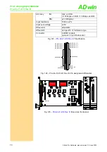
Fig. 95 – 

Pro-AIn-8/16 Rev. B

: Block diagram

Input channels

8 differential via multiplexer

Resolution

16 bit

Conversion time

max. 8µs

Sampling rate

max. 100ksps

Multiplexer settling time

14µs

Measurement ranges

±10V

Gain

1, 2, 4, 8 software selectable

Accuracy

INL

±3 LSB typical

DNL

max. ±1 LSB

Input resistance

330k

, ±2%

Input over-voltage

±17V 

Offset error

adjustable

Offset drift

±20 ppm/ºC

Connector

8 LEMO sockets
optional: 37-pin DSub socket

Fig. 96 – 

Pro-AIn-8/16 Rev. B

: Specification

ADwi

n

-Pro

 bus

A

D

MUX

1

330k
330k

2

330k
330k

8

330k
330k

. . . . . .

Addr.

Data

Data

Register

Address

Decoder

Data

PGA

Vu= 1, 2, 4, 8

. . . . .

Summary of Contents for ADwin-Pro

Page 1: ...ADwin Pro Pro II System and hardware description ADwin Pro Hardware manual version 2 9 June 2006...

Page 2: ...2 9 June 2006 J ger Computergesteuerte Messtechnik GmbH Rheinstra e 2 4 D 64653 Lorsch Germany For any questions please don t hesitate to contact us Hotline 49 6251 96320 Fax 49 6251 5 68 19 E Mail in...

Page 3: ...Analog Input Modules 23 5 4 Pro II Analog Output Modules 33 5 5 Pro I Analog Input Modules 38 5 6 Pro I Analog Output Modules 77 5 7 Pro I Analog Input and Output Modules 90 5 8 Pro I Digital I O and...

Page 4: ...rther information in this documentation or to other sources such as manuals data sheets literature etc C ADwin File names and paths are placed in angle brackets and characterized in the font Courier N...

Page 5: ...notebook previous versions used a serial link con nection In order to meet the various requirements for measurement and control tasks the system can be equipped with the following modules analog inpu...

Page 6: ...manuals Qualified personnel Programming start up and operation as well as the modification of program parameters must be performed only by appropriately qualified personnel Qualified personnel are pe...

Page 7: ...ielding on both ends for signal lines Here too you should reduce the bleeding off of interferences via the enclosure by using screen clips Supply voltage Operate the device with the defined and fittin...

Page 8: ...left edge one upper and one lower bearing Specific features for ADwin Pro II enclosures Pay attention to the color of the bearings There are different offset bearings for Pro I and Pro II modules Whi...

Page 9: ...designed for both Pro I and Pro II modules The back plane comprises the Pro I bus as well as the Pro II bus The processor module runs both buses in parallel Number of Slots 16 Main dimensions l x w x...

Page 10: ...Output modules Pro AOut x with Rev A may not be used for technical reasons The processor module must be plugged in at the middle position white bear ings There is a gap of half a slot between process...

Page 11: ...e rear of the enclosure above the power supply connector you will find a label with the revision number Number of Slots 16 Main dimensions l x w x h Slot area w x h 336mm 447 5mm 146mm 84 HP 3 U Power...

Page 12: ...Main dimensions l x w x h Slot area w x h 336mm 447 5mm 146mm 84 HP 3 U Power supply unit min 70W 100V 240VAC at 50 60Hz switching power supply Fuse 5A delayed action fuse Fig 8 Enclosure of the ADwin...

Page 13: ...a w x h 336mm 234mm 146mm 42 HP 3 U Power supply unit min 40W 100 240VAC at 50 60Hz switching power supply Fuse 2A delayed action fuse Fig 9 Enclosure ADwin Pro light Specification Revision Release Pr...

Page 14: ...0W The connector for the external power supply unit as well as a 4A fuse can be found at the rear of the ADwin Pro mini enclosure see fig 12 Fig 12 Enclosure ADwin Pro mini Rear and detail of the pin...

Page 15: ...onal group EXT special modules of all kind All Pro II modules A module address must be within the following limits Pro I modules 1 255 Pro II modules 1 15 There are special limits for RSxxx and fieldb...

Page 16: ...0 2 0 1 0 0 0 0 0 0 3 1 1 0 0 0 0 0 0 4 0 0 1 0 0 0 0 0 5 1 0 1 0 0 0 0 0 6 0 1 1 0 0 0 0 0 7 1 1 1 0 0 0 0 0 8 0 0 0 1 0 0 0 0 254 0 1 1 1 1 1 1 1 255 1 1 1 1 1 1 1 1 Fig 13 Address settings of the A...

Page 17: ...signal as trigger for an event and trigger a process that is pro cessed immediately and completely see ADbasic manual chapter Structure of the ADbasic program The event signal has to be present for 5...

Page 18: ...mory 256kB optional 512kB External memory 4MB optional 16 oder 32MB TTL signal inputs Event In Fig 17 Pro CPU T9 Specifikation DATA ADDRESS ADwin Pro bus ext Memory SRAM 3 MB DRAM 4 16 32 64 MB EVENT...

Page 19: ...ional 512kB External memory 16MB optional 64MB TTL signal inputs Event In DigIn 0 optional Fig 21 Pro CPU T9 ENET USB Specifikation Daten Adressen Daten Adressen DSP Link ADwin Pro Bus SHARC ADSP 2106...

Page 20: ...t panel LM3940IS 3 3 ADM 706 74LS125A OCX 24MHz OCX 40MHz AT17LV010 ICSI IS42S16400 7 ICSI IS42S16400 7 ICSI IS42S16400 7 ICSI IS42S16400 7 ADSP 21062 FPGA Cypress AN2135 USB Hub 24LC01B 74LVT16245 74...

Page 21: ...128MB TTL signal inputs Event In DigIn 0 Fig 25 Pro CPU T10 ENET Specifikation DATA ADDRESS DATA ADDRESS DSP LINK ADwin Pro bus SHARC ADSP 21160 from Analog Devices with 4 MBit internal SRAM ext Memor...

Page 22: ...ules be fur ther used with few but inevitable changes The processor T11 needs the include file ADwinPro_All inc to be included In parallel all other include files for Pro modules should be deleted fro...

Page 23: ...uction e g the settling time of a multiplexer with SET_MUX In this case the instruction P1_SLEEP fits for previous mod ules Pro I bus and P2_SLEEP for Pro II modules Please see the notes in the ADbasi...

Page 24: ...ink interface The boot loader unit is placed on a separate board which is located be tween the SDRAM memory and the interface circuit board The mod ule s width is 10HP and needs 2 slots in the Pro sys...

Page 25: ...analog outputs to those values which correspond to the configuration after power up normally digital 0 or 0 Volt Notes in relation to the Pro Flash Boot Please pay attention to the fact that the watc...

Page 26: ...Processor modules ADwin 22 ADwin Pro Hardware manual version 2 9 June 2006...

Page 27: ...erences may occur You can avoid open ended inputs this way Separate unused inputs from open ended lines Apply a specified level for instance GND to unused inputs Make the connection as close to the so...

Page 28: ...done by software see chapter 6 3 1 Calibration per Software The module includes a sequential control which can read measurement val ues from several or all input channels sequentially Fig 30 Pro II AI...

Page 29: ...ion 2 9 June 2006 25 Pro II Analog Input Modules Pro II AIn 8 18 L2 Rev E ADwin Fig 32 Pro II AIn 8 18 L2 Rev E Front panel AIN8 18 ANALOG INPUT 1 2 3 4 5 6 7 8 AIN AIN PE Zoom 2 pole LEMO socket seri...

Page 30: ...ro device Alterna tively a GND level signal common for all inputs can be connected to one of the AGND pins The ground connection to the Pro device should be split up by switching the DIL switch see fi...

Page 31: ...naloger Eingang 15 Analoger Eingang 16 AGND 5V AGND 19 18 17 16 15 14 13 12 11 10 9 8 7 6 5 4 3 2 1 37 36 35 34 33 32 31 30 29 28 27 26 25 24 23 22 21 20 Analoger Eingang 1 Analoger Eingang 2 Analoger...

Page 32: ...by software see chapter 6 3 1 Calibra tion per Software As an option the module can return the moving average of 2 32 measure ment values instead of simple measurement values Burst Sequence The modul...

Page 33: ...idth 0 4MHz Memory size 256MB or 227 134217728 values total Measurement range 10V with max offset 3 5 V Accuracy INL typical 1 2 LSB max 5 LSB DNL typical 0 5 LSB max 1 LSB Input resistance 330k 2 Inp...

Page 34: ...8 ENABLE diff RS422 B diff RS422 AGND EVENT A diff RS422 ANALOG IN 1 ANALOG IN 2 ANALOG IN 3 ANALOG IN 4 ANALOG IN 5 ANALOG IN 6 ANALOG IN 7 ANALOG IN 8 ENABLE diff RS422 B diff RS422 AGND RESERVED EV...

Page 35: ...input voltage range of 10V The adjustment of gain and offset is made by software see chapter 6 3 1 Calibra tion per Software Fig 42 Pro II AIn F 8 18 Rev E Block diagram Input channels 8 differential...

Page 36: ...IN 5 ANALOG IN 6 ANALOG IN 7 ANALOG IN 8 ENABLE Opto 5V AGND EVENT A Opto 5V ANALOG IN 1 ANALOG IN 2 ANALOG IN 3 ANALOG IN 4 ANALOG IN 5 ANALOG IN 6 ANALOG IN 7 ANALOG IN 8 ENABLE Opto 5V AGND RESERV...

Page 37: ...This section describes analog input modules for ADwin Pro II Analog output modules for ADwin Pro I be found from page 77 Module name AOut 4 16 AOut 8 16 Revision E E Number DAC 4 8 Resolution bit 16...

Page 38: ...4 16 D DSub socket 37 pin Modules with DSub socket have an event input an event given may be for warded as trigger signal to the processor module Fig 46 Pro II AOut 4 16 Rev E Block diagram Output cha...

Page 39: ...Fig 48 Pro II AOut 4 16 Rev E Pin assignment DSub and front cover ANALOG OUT 1 ANALOG OUT 2 ANALOG OUT 3 ANALOG OUT 4 DGND 19 18 17 16 15 14 13 12 11 10 9 8 7 6 5 4 3 2 1 37 36 35 34 33 32 31 30 29 2...

Page 40: ...o II AOut 8 16 D DSub socket 37 pin Modules with DSub socket have an event input an event given may be for warded as trigger signal to the processor module Fig 49 Pro II AOut 8 16 Rev E Block diagram...

Page 41: ...Pin assignment DSub and front cover ANALOG OUT 1 ANALOG OUT 2 ANALOG OUT 3 ANALOG OUT 4 ANALOG OUT 5 ANALOG OUT 6 ANALOG OUT 7 ANALOG OUT 8 DGND 19 18 17 16 15 14 13 12 11 10 9 8 7 6 5 4 3 2 1 37 36...

Page 42: ...5 0 75 0 5 8 5 0 75 0 5 0 5 10 8 5 8 5 0 75 0 75 0 4 0 4 8 8 max sampl rate ksample s 117 a a To be achieved under favorable conditions 1 input channel time optimized program 1250 a 2000 117 a 1250 a...

Page 43: ...d inputs Open ended inputs can cause errors above all in an environment where inter ferences may occur You can avoid open ended inputs this way Separate unused inputs from open ended lines Apply a spe...

Page 44: ...he module can be combined with amplifiers filters thermocouples and PTC modules The input voltage range can be selected by jumpers see page 41 Fig 52 Pro AIn 8 12 Rev A Block diagram Input channels 8...

Page 45: ...as well as GAIN are available fig 57 ANALOG IN 1 ANALOG IN 2 ANALOG IN 3 ANALOG IN 4 ANALOG IN 5 ANALOG IN 6 ANALOG IN 7 ANALOG IN 8 AGND RESERVED ANALOG IN 1 ANALOG IN 2 ANALOG IN 3 ANALOG IN 4 ANALO...

Page 46: ...AIn 8 12 Rev B is an advanced development of the module Pro AIn 8 12 Rev A with an input voltage range of 10V or 0 10V and a gain programmable by software of 1 2 4 or 8 The adjustment of gain and offs...

Page 47: ...6 3 1 Calibration per Software page 194 ANALOG IN 1 ANALOG IN 2 ANALOG IN 3 ANALOG IN 4 ANALOG IN 5 ANALOG IN 6 ANALOG IN 7 ANALOG IN 8 AGND RESERVED ANALOG IN 1 ANALOG IN 2 ANALOG IN 3 ANALOG IN 4 A...

Page 48: ...ware see chapter 6 3 1 Calibration per Software The module includes a sequence control which may read the measurement values of all input channel sequentially Fig 63 Pro AIn 8 14 Rev A Block diagram I...

Page 49: ...N 6 ANALOG IN 7 ANALOG IN 8 AGND RESERVED DGND 19 18 17 16 15 14 13 12 11 10 9 8 7 6 5 4 3 2 1 37 36 35 34 33 32 31 30 29 28 27 26 25 24 23 22 21 20 RESERVED RESERVED 19AD0202 A0 A1 A2 A3 A4 A5 A6 A7...

Page 50: ...32 12 Rev A Block diagram After power up the module Pro AIn 32 12 is set to 16 differential inputs The figures 69 and 70 show the pin assignment of the module Please consider the different pin assign...

Page 51: ...ANALOG IN 18 ANALOG IN 19 ANALOG IN 20 ANALOG IN 21 ANALOG IN 22 ANALOG IN 23 ANALOG IN 24 ANALOG IN 25 ANALOG IN 26 ANALOG IN 27 ANALOG IN 28 ANALOG IN 29 ANALOG IN 30 ANALOG IN 31 ANALOG IN 32 AGND...

Page 52: ...range J1 J2 5V bipolar BIP 10V 10V bipolar default BIP 20V 0 10V unipolar UNI 10V not allowed 0 20V UNI 20V Fig 72 Pro AIn 32 12 Rev A Jumper positions Potenti ometer Adjustment of Gain Gain factor B...

Page 53: ...2 4 or 8 The adjustment of gain and offset is made by software see chapter 6 3 1 Calibration per Software Fig 74 Pro AIn 32 12 Rev B Block diagram After power up the module is set to 16 differential...

Page 54: ...5 ANALOG IN 6 ANALOG IN 7 ANALOG IN 8 ANALOG IN 9 ANALOG IN 10 ANALOG IN 11 ANALOG IN 12 ANALOG IN 13 ANALOG IN 14 ANALOG IN 15 ANALOG IN 16 AGND RESERVED DGND 19 18 17 16 15 14 13 12 11 10 9 8 7 6 5...

Page 55: ...sequential control which by request reads the measurement values from all input channels successively Fig 80 Pro AIn 16 14 C Rev A Block diagram Input channels 16 differential Resolution 14 bit Conver...

Page 56: ...G IN 4 ANALOG IN 5 ANALOG IN 6 ANALOG IN 7 ANALOG IN 8 ANALOG IN 17 ANALOG IN 18 ANALOG IN 19 ANALOG IN 20 ANALOG IN 21 ANALOG IN 22 ANALOG IN 23 ANALOG IN 24 AGND RESERVED DGND 19 18 17 16 15 14 13 1...

Page 57: ...request reads the measurement values from all input channels successively Fig 84 Pro AIn 32 14 Rev A Block diagram After power up the module is set to 16 differential inputs Figures 86 and 87 show th...

Page 58: ...33 32 31 30 29 28 27 26 25 24 23 22 21 20 ANALOG IN 1 ANALOG IN 2 ANALOG IN 3 ANALOG IN 4 ANALOG IN 5 ANALOG IN 6 ANALOG IN 7 ANALOG IN 8 ANALOG IN 17 ANALOG IN 18 ANALOG IN 19 ANALOG IN 20 ANALOG IN...

Page 59: ...DSub socket 37 pin The input voltage range of the ADC can be adjusted by jumpers see below Fig 89 Pro AIn 8 16 Rev A Block diagram Input channels 8 differential via multiplexer Resolution 16 bit Conve...

Page 60: ...ALOG IN 2 ANALOG IN 3 ANALOG IN 4 ANALOG IN 5 ANALOG IN 6 ANALOG IN 7 ANALOG IN 8 AGND RESERVED ANALOG IN 1 ANALOG IN 2 ANALOG IN 3 ANALOG IN 4 ANALOG IN 5 ANALOG IN 6 ANALOG IN 7 ANALOG IN 8 AGND RES...

Page 61: ...t of the module Pro AIn 8 16 with an input voltage range of 10V and a gain programmable by software of 1 2 4 or 8 The adjustment of gain and offset is made by soft ware see chapter 6 3 1 Calibration p...

Page 62: ...RESERVED ANALOG IN 1 ANALOG IN 2 ANALOG IN 3 ANALOG IN 4 ANALOG IN 5 ANALOG IN 6 ANALOG IN 7 ANALOG IN 8 AGND RESERVED DGND 19 18 17 16 15 14 13 12 11 10 9 8 7 6 5 4 3 2 1 37 36 35 34 33 32 31 30 29...

Page 63: ...djustment of gain and offset is made by software see chapter 6 3 1 Calibration per Software In addition the module has a sequential control which by request reads the measurement values from all input...

Page 64: ...D RESERVED ANALOG IN 1 ANALOG IN 2 ANALOG IN 3 ANALOG IN 4 ANALOG IN 5 ANALOG IN 6 ANALOG IN 7 ANALOG IN 8 AGND RESERVED DGND 19 18 17 16 15 14 13 12 11 10 9 8 7 6 5 4 3 2 1 37 36 35 34 33 32 31 30 29...

Page 65: ...is made by software see chapter 6 3 1 Calibration per Soft ware Fig 103 Pro AIn 32 16 Rev B Block diagram On Startup the module is set to 16 differential inputs Figures 105 and 106 show the pin assign...

Page 66: ...RESERVED DGND 19 18 17 16 15 14 13 12 11 10 9 8 7 6 5 4 3 2 1 37 36 35 34 33 32 31 30 29 28 27 26 25 24 23 22 21 20 ANALOG IN 1 ANALOG IN 2 ANALOG IN 3 ANALOG IN 4 ANALOG IN 5 ANALOG IN 6 ANALOG IN 7...

Page 67: ...ntrol which by request reads the measurement values from all input channels successively Fig 108 Pro AIn 32 16 Rev C Block diagram On Startup the module is set to 16 differential inputs Figures 110 an...

Page 68: ...RESERVED DGND 19 18 17 16 15 14 13 12 11 10 9 8 7 6 5 4 3 2 1 37 36 35 34 33 32 31 30 29 28 27 26 25 24 23 22 21 20 ANALOG IN 1 ANALOG IN 2 ANALOG IN 3 ANALOG IN 4 ANALOG IN 5 ANALOG IN 6 ANALOG IN 7...

Page 69: ...ders for the num ber of the corresponding ADC The potentiometer names are imprinted on the board Fig 113 Pro AIn F 4 12 Rev A Block diagram Input channels 4 differential Resolution 12 bit Conversion t...

Page 70: ...4 AGND RESERVED ANALOG IN 1 ANALOG IN 2 ANALOG IN 3 ANALOG IN 4 AGND RESERVED DGND 19 18 17 16 15 14 13 12 11 10 9 8 7 6 5 4 3 2 1 37 36 35 34 33 32 31 30 29 28 27 26 25 24 23 22 21 20 RESERVED RESER...

Page 71: ...the accurate adjustment on page 68 Fig 117 Pro AIn F 8 12 Rev A Block diagram Input channels 8 differential Resolution 12 bit Conversion time max 0 75 s per ADC Sampling rate max 1250ksps per ADC Mea...

Page 72: ...tentiometers have been optimally adjusted Therefore we ask you to avoid adjusting the potentiometers if not necessary because this may result in inaccuracy The calibration of the ADC is described in t...

Page 73: ...asurement frequency are to be defined in the program are stored in a special burst memory of the module which enables measurement frequencies of up to 2MHz The size of the burst memory limits the numb...

Page 74: ...ication ANALOG IN 1 ANALOG IN 2 ANALOG IN 3 ANALOG IN 4 AGND RESERVED ANALOG IN 1 ANALOG IN 2 ANALOG IN 3 ANALOG IN 4 AGND RESERVED DGND 19 18 17 16 15 14 13 12 11 10 9 8 7 6 5 4 3 2 1 37 36 35 34 33...

Page 75: ...ues number and measurement frequency are to be defined in the program are stored in a special burst memory of the module which enables measurement frequencies of up to 2MHz The size of the burst memor...

Page 76: ...ED ANALOG IN 1 ANALOG IN 2 ANALOG IN 3 ANALOG IN 4 ANALOG IN 5 ANALOG IN 6 ANALOG IN 7 ANALOG IN 8 AGND RESERVED DGND 19 18 17 16 15 14 13 12 11 10 9 8 7 6 5 4 3 2 1 37 36 35 34 33 32 31 30 29 28 27 2...

Page 77: ...The x of the potentiometer s names are place holders for the num ber of the corresponding ADC The potentiometer names are imprinted on the board Fig 130 Pro AIn F 4 16 Rev A Block diagram Input chann...

Page 78: ...4 AGND RESERVED ANALOG IN 1 ANALOG IN 2 ANALOG IN 3 ANALOG IN 4 AGND RESERVED DGND 19 18 17 16 15 14 13 12 11 10 9 8 7 6 5 4 3 2 1 37 36 35 34 33 32 31 30 29 28 27 26 25 24 23 22 21 20 RESERVED RESER...

Page 79: ...on page 68 The x of the potentiometer s names are place holders for the num ber of the corresponding ADC The potentiometer names are imprinted on the board Fig 134 Pro AIn F 8 16 Rev A Block diagram...

Page 80: ...3 ANALOG IN 4 ANALOG IN 5 ANALOG IN 6 ANALOG IN 7 ANALOG IN 8 AGND RESERVED DGND 19 18 17 16 15 14 13 12 11 10 9 8 7 6 5 4 3 2 1 37 36 35 34 33 32 31 30 29 28 27 26 25 24 23 22 21 20 RESERVED RESERVE...

Page 81: ...AOut 4 16 M2 AOut 8 16 AOut 8 16 AOut 8 16 Rev A B C A B C No ADC 4 4 4 8 8 8 Resolution bit 16 16 16 16 16 16 max settling time s 20 3 3 3 20 3 3 3 Channels sng end 4 4 4 8 8 8 Voltage range 5V x x x...

Page 82: ...cket 37 pin Jumpers are used to set the output voltage range of the DAC see page 81 Fig 138 Pro AOut 4 16 Rev A Block diagram Output channels 4single ended Resolution 16 bit Settling time to 0 01 FSR...

Page 83: ...ND 19 18 17 16 15 14 13 12 11 10 9 8 7 6 5 4 3 2 1 37 36 35 34 33 32 31 30 29 28 27 26 25 24 23 22 21 20 RESERVED AGND RESERVED 19DA714 FPGA FPGA ON 1 2 3 4 5 6 7 8 A0 A1 A2 A3 A4 A5 A6 A7 LS19 OCX DC...

Page 84: ...D DSub socket 37 pin Jumpers are used to set the output voltage range of the DAC see page 81 Fig 142 Pro AOut 8 16 Rev A Block diagram Output channels 8 single ended Resolution 16 bit Settling time t...

Page 85: ...ntiometers The potentiometers U0x Bx and Gainx are used for an accurate adjustment of gain and offset fig 147 If nothing else has been said on ordering the module the voltage range is set to 10V After...

Page 86: ...bipolar BIP 10V 10V bipolar default BIP 20V 0 10V unipo lar UNI 10V not allowed 0 20V UNI 20V Fig 146 Pro AOut 8 16 Rev A Jumper positions for the output voltage range Potenti ometer Adjustment of Ga...

Page 87: ...kets CAMAC European norm The output voltage range of the DAC can be set by two DIL switches see page 84 The adjustment of gain and offset is made by software see chapter 6 3 1 Calibration per Software...

Page 88: ...OUT 1 ANALOG OUT 2 ANALOG OUT 3 ANALOG OUT 4 DGND 19 18 17 16 15 14 13 12 11 10 9 8 7 6 5 4 3 2 1 37 36 35 34 33 32 31 30 29 28 27 26 25 24 23 22 21 20 RESERVED AGND RESERVED ANALOG OUT 1 ANALOG OUT...

Page 89: ...ADC in order to assure good measurement results 19DA0101 A0 A1 A2 A3 A4 A5 A6 A7 DC DC converter 74LS19 ON DIP 1 2 3 4 5 6 7 8 OPA 2132 OPA 2132 AD588BQ OPA 2132 OPA 2132 OPA 2132 OPA 2132 LT 1468 LTC...

Page 90: ...rsion M2 the module has an additional internal memory SRAM of 2MB for a function generator In the memory data any wave forms are stored which the function generator outputs with a specified output fre...

Page 91: ...9 8 7 6 5 4 3 2 1 37 36 35 34 33 32 31 30 29 28 27 26 25 24 23 22 21 20 RESERVED AGND RESERVED DC DC converter A0 A1 A2 A3 A4 A5 A6 A7 ON DIP 1 2 3 4 5 6 7 8 AD588 OPA 2132 OPA 2132 10V 5V BIP UNI UNI...

Page 92: ...ors Pro AOut 8 16 shielded LEMO sockets CAMAC European norm Pro AOut 8 16 D DSub socket 37 pin Fig 159 Pro AOut 8 16 Rev C Block diagram Output channels 8 single ended Resolution 16 bit Settling time...

Page 93: ...22 21 20 AGND RESERVED RESERVED DC DC converter A0 A1 A2 A3 A4 A5 A6 A7 ON DIP 1 2 3 4 5 6 7 8 AD588 OPA 2132 OPA 2132 OPA 2132 OPA 2132 10V 5V BIP UNI UNI BIP 5V 10V INA 154 INA 154 LT 1468 LTC1597...

Page 94: ...ll as in the group of the analog output modules Fig 163 Pro AO 16 8 12 Rev A Block diagram Fig 164 Pro AO 16 8 12 Rev A Pin assignment Data ADwin Pro bus A D 1 100k 100k 100k Addr Data Data Register A...

Page 95: ...ctable Accuracy INL max 1 LSB DNL max 1 LSB Input resistance 100k 2 Input over voltage 35V Offset error adjustable Offset drift 30 ppm C of full scale range DAC Output channels 8 single ended Resoluti...

Page 96: ...G1 4 and G5 8 fig 170 are used for an accurate adjustment of gain and offset The jumpers as well as the potentiometers for setting the output voltage range can be found on the lower part of the module...

Page 97: ...Flash card hard disk from ADbasic With integrated real time clock 142 Module Rev Chan nels Counter Input voltage UIn Isolation V Page No Typea Resol Bit V Type CNT VR4 CNT VR4 L A 4 1 UD 32 5 TTL 104...

Page 98: ...d front panel ADwin Pro bus 0 1 31 2 3 30 EVENT Data Register Data 10k 10k 10k 10k 10k 10k 10k DIG I O BIT 1 DIG I O BIT 3 DIG I O BIT 5 DIG I O BIT 7 DIG I O BIT 9 DIG I O BIT 11 DIG I O BIT 13 DIG I...

Page 99: ...via software as input or output Digital inputs TTL logic Pull Down Resistor 10k VIH min 2 4V VIL max 0 8V IIH max 0 55mA IIL max 0 01mA Voltage range 0 5V 5 5V Output current max 6mA per channel outpu...

Page 100: ...Block diagram Fig 176 Pro DIO 32 Rev B Pin assignment ADwin Pro bus 0 1 31 2 3 30 EVENT Data Register Data 10k 10k 10k 10k 10k 10k 10k Bus Trans ceiver D00 07 Bus Trans ceiver D08 15 Bus Trans ceiver...

Page 101: ...n 2V VIL max 0 8V IIH max 1 A IIL max 0 01mA Voltage range 0 5V 5 5V Output current max 35mA per channel max 70mA per block 8 channels via VCC or GND Event input TTL logic Power up status All channels...

Page 102: ...well Fig 179 Pro OPT 16 Rev A Block diagram Fig 180 Pro OPT 16 Rev A Pin assignment ADwin Pro bus 0 15 Data Register Data EVENT 1k51 1k 510 24V 12V 5V 1k51 1k 510 24V 12V 5V 1k51 1k 510 24V 12V 5V DI...

Page 103: ...voltage 5V 8V 5V 16V 5V 30V Switching time 200ns Isolation 42V channel channel channel GND Connector 37 pin DSub socket Fig 182 Pro OPT 16 Rev A Specification 19OPT01 FPGA FPGA ON 1 2 3 4 5 6 7 8 A0...

Page 104: ...d and front panel ADwin Pro bus A B 0 Data EVENT 4k3 2k 560 24V 12V 5V Data Register A B 15 RELAY 0 A RELAY 1 A RELAY 2 A RELAY 3 A RELAY 4 A RELAY 5 A RELAY 6 A RELAY 7 A RELAY 8 A RELAY 9 A RELAY 10...

Page 105: ...00mA per channel Contact 1 per channel normally open optional normally closed Operate time 4ms Release time 3ms Bounce time 2ms Event inputs 1 Isolation 42V channel channel chan nel GND Event input vo...

Page 106: ...k 56k 56k 1N 4001 BC489 Vcc GND VEE 0 VEE 15 VCC GND DGND EVENT IN EMITTER 0 EMITTER 1 EMITTER 2 EMITTER 3 EMITTER 4 EMITTER 5 EMITTER 6 EMITTER 7 EMITTER 8 EMITTER 9 EMITTER 10 EMITTER 11 EMITTER 12...

Page 107: ...hing voltage 5 30V DC with external power supply Switching current 200mA max per channel Voltage drop 0 5V Switching time 10 s Event input 1 Isolation 42V channel channel channel GND Event input volta...

Page 108: ...each counter indi vidually According to the mode of operation either the inputs A B are active or the inputs CLK DIR Fig 191 Pro CNT VR4 Rev A Block diagram The module Pro CNT VR4 Rev A is also avail...

Page 109: ...IR CNTR 2 B CNTR 3 DIR CNTR 3 B CNTR 4 DIR CNTR 4 B DGND EVENT IN CNTR 1 CLR CNTR 1 CLK CNTR 1 A RESERVED CNTR 2 CLR CNTR 2 CLK CNTR 2 A RESERVED CNTR 3 CLR CNTR 3 CLK CNTR 3 A RESERVED CNTR 4 CLR CNT...

Page 110: ...e selected by jumpers The default setting of the input voltage range is 24V The counter inputs are optically isolated from the system circuitry as well as from other inputs The event input is also iso...

Page 111: ...R RESERVED CNTR 2 A CLK CNTR 2 B DIR CNTR 2 CLR RESERVED CNTR 3 A CLK CNTR 3 B DIR CNTR 3 CLR RESERVED CNTR 4 A CLK CNTR 4 B DIR CNTR 4 CLR EVENT IN 19 18 17 16 15 14 13 12 11 10 9 8 7 6 5 4 3 2 1 37...

Page 112: ...nce between two successive register val ues Since the register access is discrete time the frequency can be calcu lated online Fig 203 Pro CNT 8 32 Rev A Block diagram The module Pro CNT 8 32 Rev A is...

Page 113: ...te 10MHz max Signal pulse width min 50ns Inputs TTL Trigger Input pos TTL Pull down resistor 10k VIH min 2 4V VIL max 0 8V IIH max 0 55mA IIL max 0 01mA Voltage range absolute 0 3V 7V Connector 37 pin...

Page 114: ...from the system circuitry as well as from other inputs The event input is also isolated from the system circuitry The input voltage range can be selected by three jumpers The default setting of the i...

Page 115: ...nnector 37 pin DSub socket Isolation 42V channel channel channel GND Fig 210 Pro CNT 8 32 I Rev A Specification 19CNT01 ON 1 2 3 4 5 6 7 8 A0 A1 A2 A3 A4 A5 A6 A7 FPGA FPGA 74ABT16245 74LS19 74LS19 74...

Page 116: ...ence of two successive readings of the latch Fig 211 Pro CNT 16 16 Rev A Block diagram The module Pro CNT 16 16 Rev A is equipped with 16 times the components shown in the block diagram exception the...

Page 117: ...rate 10MHz max Signal pulse width min 50ns Inputs TTL Trigger Input pos TTL Pull down resistor 10k VIH min 2 4V VIL max 0 8V IIH max 1mA IIL max 0 2mA Voltage range absolute 0 3V 7V Connector 37 pin D...

Page 118: ...nput is also isolated from the system circuitry The input voltage range can be selected by jumpers The default setting of the input voltage range is 24V Fig 215 Pro CNT 16 16 I Rev A Block diagram The...

Page 119: ...nnector 37 pin DSub socket Isolation 42V channel channel channel GND Fig 218 Pro CNT 16 16 I Rev A Specification 19CNT01 ON 1 2 3 4 5 6 7 8 A0 A1 A2 A3 A4 A5 A6 A7 FPGA FPGA 74ABT16245 74LS19 74LS19 7...

Page 120: ...e time the frequency can be calculated online Fig 219 Pro CNT 16 32 Rev A Block diagram The module Pro CNT 16 32 Rev A is equipped with 16 times the components shown in the block diagram exception the...

Page 121: ...min 25ns Inputs TTL Trigger Input pos TTL Pull down resistor 10k VIH min 2 4V VIL max 0 8V IIH max 1mA IIL max 0 2mA Voltage range absolute 0 3V 7V Connector 37 pin DSub socket Isolation No see page...

Page 122: ...try The input voltage range can be selected by jumpers The default setting of the input voltage range is 24V Fig 223 Pro CNT 16 32 I Rev A Block diagram The module Pro CNT 16 32 I Rev A is equipped wi...

Page 123: ...ching time 200ns Connector 37 pin DSub socket Isolation 42V channel channel channel GND Fig 226 Pro CNT 16 32 I Rev A Specification 19DIOCNT201 A0 A1 A2 A3 A4 A5 A6 A7 OCX 40MHz AT17LV010 LM3940 3 3 X...

Page 124: ...1st and 2nd counter of the module CNT VR4 and the 1st and 2nd PW counter is related to the 3rd and 4th counter of the module CNT PW4 CNTR 1 DIR CNTR 1 B CNTR 2 DIR CNTR 2 B DGND EVENT IN CNTR 1 CLR C...

Page 125: ...eriod width of the highest input frequency to be measured Example The signal whose positive and negative pulse widths you want to know has a frequency of 3 3kHz The event has to arrive in a time inter...

Page 126: ...T PW4 Rev A Allocation of the latches Counter 4 impulse counters Counter resolution 32 bit Reference clock 5MHz Inputs 4 TTL VIH min 2 4V VIL max 0 8V IIH max 20 A IIL max 50 A Voltage range 0 3V 7V E...

Page 127: ...er value will be stored in two separate latches Please make sure that the delay of the event via internal or external timer is smaller than the period width of the highest input frequency to be measur...

Page 128: ...es resistor 560 2k 4 3k Input over voltage 8V 16V 30V Negative voltage 5V for all ranges Switching time 200ns Isolation 42V channel channel channel GND Connector 37 pin DSub socket Fig 238 Pro CNT PW4...

Page 129: ...by getting the difference of two read latch values because this difference defines the number of pulses between the two reading processes PWM analysis With the PWM analysis the signal which is to be...

Page 130: ...sis 40MHz Connector 37 pin DSub socket Power consumption approx 150mA Isolation No see page 127 Fig 242 Pro CO4 T Rev A Specification 19DIOCNT0101 A0 A1 A2 A3 A4 A5 A6 A7 OCX 40MHz LTC485 AT17LV010 LM...

Page 131: ...ic Control registers 32 bit Latch 1 4 CLK EN CLR A CLK PWM B DIR CLR LATCH DIR DIR EVENT 12V 5V 24V 12V 5V 24V 12V 5V 24V 12V 5V 24V 32 bit Latch 9 12 CO4_CLEAR CO4_LATCHENABLE CO4_CLEARENABLE CO4_SET...

Page 132: ...put over voltage 8V 16V 30V Negative voltage 5V for all ranges Switching time 100ns Isolation 42Vchannel channel channel GND Connector 37 pin DSub socket Power consumption approx 200mA 1 A low high si...

Page 133: ...d have RS422 485 levels The clock rates as well as the resolution of the encoder up to 32 bits are pro grammable via pre scaler of approx 40kHz to 1MHz A conversion from gray into binary code is made...

Page 134: ...ure below illustrates the DIP switch positions and the resulting input counter connections Program one of the two counters with CLK and DIR signal inputs up down counter the other with PWM input PWM a...

Page 135: ...or 37 pin DSub socket Power consumption approx 200mA Fig 252 Pro CO4 D Rev A Specification DIP switch position Inputcounter A CLK PWM Counter CNTR 1 CNTR 2 CNTR 3 CNTR 4 Fig 250 Pro CO4 D Rev A Alloca...

Page 136: ...the PWM output putting it into a static mode This can only be made by the command PWM_OUT which sets the output to a defined status when the counter is enabled The lowest output frequency at a still d...

Page 137: ...PWM channels Outputs TTL Counter register width 16 bit fclk after Prescaler Div by 1 20 200ns 5MHz Div by 2 21 400ns 2 5MHz Div by 4 22 800ns 1 25MHz Div by 128 27 25 6 s 39kHz VOH 2 4V min VOL 0 8V...

Page 138: ...well The input voltage range of the counter inputs can be selected by jumpers The default setting of the input voltage range is 24V By setting a register the counters can be enabled or disabled But do...

Page 139: ...e 5V 12V 24V selectable via jumpers Connector 37 pin DSub socket Isolation 42V channel channel channel GND Fig 260 Pro PWM 4 I Rev A Specification RESERVED EVENT IN PWM OUTPUT 1 PWM OUTPUT 2 PWM OUTPU...

Page 140: ...ency Instructions for the PWM modules PWM_SET PWM_SET does the settings of the defined module for the prescaler and the duration of the high and low pulses of the PWM output channel PWM_SET module cha...

Page 141: ...C ADwin ADbasic3 Samples_ADwin_Pro generates identical PWM signals at the outputs 1 4 with a frequency of 1kHz With the parameters PAR_1 PAR_14 you will be able to change in ADbasic the following valu...

Page 142: ...hannels The current converted measurement values The maximum and minimum of the acquired measurement values The last 1024 measurement values of 2 selected channels The digital signals 1 0 of measureme...

Page 143: ...1 7S08 AD9201ARS DC DC converter 24LC01B AD8056AN AD8056AN AD8056AN AD8056AN AD8056AN AD8056AN AD8056AN AD8056AN AD9201ARS AD9201ARS AD9201ARS AD9201ARS AD9201ARS AD9201ARS AD9201ARS 19ADC0103 COMP 16...

Page 144: ...a a global memory FIFO A standard example for such a low priority pro cess is included in delivery illustrating how to write data to the storage medium The further module description is into the follo...

Page 145: ...status of the storage medium The top and lower right LEDs are individually programmable see ADbasic instruction SETLED The Real Time Clock The module is equipped with a real time clock from Epson RTC...

Page 146: ...e time must be specified by a valid date and time of day it has a resolution of one second Leap years are considered The clock is battery backed and can remain up to 2 years without any external power...

Page 147: ...fic In user specific writing reading processes low efficiency Hard disks Longer breaks between writing and reading sequences Hard disks turn into sleep mode after some seconds for the exact value see...

Page 148: ...erated on the storage medium into which the data is written During initialization the final size of the files is defined The file information is stored twice so that the file manage ment accesses the...

Page 149: ...ose module The modules differ from each other in the spec ified module address see Setting the module s addresses on page 11 Select a Pro Storage module and confirm with OK Read file structure If the...

Page 150: ...1 024 byte The value Free Size bottom right under Info indicates how many kilobytes can still be used on the storage medium The column Size on Disk indicates how many kilobytes the file needs on the...

Page 151: ...file FILEINFO DAT This information is used for the file management on the ADwin system In sector 2 absolute the start and end sectors are saved in the file FILEINFO DAT the current relative write and...

Page 152: ...es how many data of the file are copied to the PC Total Filesize saves the whole file including the data sectors where nothing is written into File data only saves only the data sector where data has...

Page 153: ...be transferred The amount of data must not be higher than the size of the destination file Confirm the selection by clicking on Open The dialog box closes and a bar in another window shows the status...

Page 154: ...ructure and manage ment which is already installed on the storage medium adjust the timing of processes The fact that 2 or more processes are running synchronously requires that you coordinate the tim...

Page 155: ...the basic parameters Either the first process or the PC start the second process Measurement process starts Flexible If the MP starts the SP it can re define the number of the destination file the ti...

Page 156: ...tes data into the FIFO array f_cmd 1 Number 1 10 of the file f_cmd 2 Write mode in the SP 0 Write data starting at the beginning of the file New means to overwrite previous data 1 Append data at the e...

Page 157: ...ds the cycle time of the MP to the cycle time of the SP Globaldelay It may be necessary to change the size of the data FIFO DATA_199 additionally to the cycle time to get the necessary results The SP...

Page 158: ...are principally used for the non time critical exchange of data of a specific length If you do prefer a data process with faster access times call our support hot line Rules of importance The followin...

Page 159: ...ocouple amplifier Type J 0 C 750 C K 200 C 950 C Accuracy in bits 12 Channels 4 8 16 Page 157 Module PT100 4 PT100 8 Revision A A Type RTD amplifier Version 2 3 or 4 wires Temperature range 200 C 266...

Page 160: ...NL 1 CAN 2 CANL 2 Revision A A A A Type CAN interface CAN Version High speed Low speed High speed Low speed Interfaces 1 2 Page 157 Module PROFI DP SL Inter SL Revision A A Type Fieldbus interface Fie...

Page 161: ...24 23 22 21 20 RESERVED RESERVED Fig 271 Pro TC 8 Rev A Block diagram Fig 272 Pro TC 8 x D Rev A Pin assignment differential ADwin Pro bus 1 2 8 Addr Address Decoder TC Amp ice point comp TC Amp ice p...

Page 162: ...e information Fig 276 Pro TC 4 J Rev A Board and front panel Input channels Pro TC 4 4 Pro TC 8 8 Pro TC 16 16 Multiplexer settling time 50 s Type measurement range J 0 C 750 C K 200 C 950 C Output vo...

Page 163: ...8 Pro TC 16 K D Rev A Board and front panel FPGA ON 1 2 3 4 5 6 7 8 A0 A1 A2 A3 A4 A5 A6 A7 DC DC Wandler MPC506AU AD595 AD595 AD595 AD595 AD595 AD595 AD595 AD595 TC8 K A OUT 1 2 3 4 5 6 7 8 TC INPUT...

Page 164: ...e As soon as a value is queried via software the module calculates the thermoelec tric voltage or the temperature in Celsius or Fahrenheit from the last mea surement value All calculation is based upo...

Page 165: ...2006 161 Pro I Signal Conditioning and Interface Modules Pro TC 8 ISO Rev A ADwin Fig 281 Pro TC 8 ISO Rev A Board and front panel ON DIP 1 2 3 4 5 6 7 8 GND OFF GND OFF GND OFF GND OFF GND OFF GND OF...

Page 166: ...oint and gain are set via jumpers and trimmers on the circuit board page 166 The measuring methods and the wiring between senso and Pro PT100 mod ule is described on page 165 Fig 282 Pro PT100 x Rev A...

Page 167: ...UT 15V 65mA PT100 8 RTD INPUT A OUT 1 2 3 4 5 6 7 8 19PT02 FPGA ON 1 2 3 4 5 6 7 8 A0 A1 A2 A3 A4 A5 A6 A7 OPA 132U MPC506AU REF 102U OPA 2132U 2 4L 3L INA 132U OPA 27U INA 118U INA 132U INA 132U 2 4L...

Page 168: ...65mA PT100 4 RTD INPUT A OUT Fig 289 Pro PT100 8 D Pin assignment Fig 290 Pro PT100 4 D Pin assignment 1 2 3 4 Source Source Sense Sense SENSOR 1 SOURCE 1 SENSOR 2 SOURCE 2 SENSOR 3 SOURCE 3 SENSOR 4...

Page 169: ...nector Connect source pin 4 with sensor pin 1 LEMO connector Connect source pin 3 with sensor pin 2 Set the jumper on the PCB to the position 2 4L 3 wire 3 wire measurement In order to avoid the disad...

Page 170: ...per position 2 4L 2 or 4 wire measurement Lower position 3L 3 wire measurement The zero point at 0 C is set with the trimmers OFFSET 1 to OFFSET 8 the scale factor or gain with GAIN 1 to GAIN 8 Fig 29...

Page 171: ...low pass filter module and an ana log input module are then forming one unity which is 2 inches 10 HP wide and therefore needs two slots The switching from sample to hold mode has to be made by the in...

Page 172: ...is available with the following connectors Pro MB8 DD Inputs and outputs with DSub sockets Pro MB8 DD Inputs DSub socket outputs LEMO sockets Pro MB8 DD Inputs LEMO sockets outputs DSub socket Pro MB...

Page 173: ...NSOR 8 EXCITATION 8 SENSOR 1 EXCITATION 1 SENSOR 2 EXCITATION 2 SENSOR 3 EXCITATION 3 SENSOR 4 EXCITATION 4 SENSOR 5 EXCITATION 5 SENSOR 6 EXCITATION 6 SENSOR 7 EXCITATION 7 SENSOR 8 EXCITATION 8 19 1...

Page 174: ...by 15 message objects The 255 registers are used for configuration and status display of the CAN con troller Here the bus speed and interrupt handling etc are set see separate documentation 82527 Seri...

Page 175: ...H CAN controller intel 82527 EVENT CAN Trans ceiver 82C250 CANL Data CANH CAN controller intel 82527 EVENT CAN Trans ceiver 82C250 CANL Data 19CAN01 OCX FPGA ON DIP 1 2 3 4 5 6 7 8 CAN Controller 8252...

Page 176: ...sage objects The message objects can either be configured to send or to receive messages Message object 15 can only be used to receive messages After initializing the CAN controller all message object...

Page 177: ...additional buffer so that 2 messages can be stored there Assigning messages The allocation of an arriving message to a message object is automatically controlled by comparing its identifiers The globa...

Page 178: ...d below The following table shows the admitted values and the meaning of the individ ual ranges The default setting of the ranges SJW and SPL is 0 and should only be changed if necessary Select the sa...

Page 179: ...upt the register is set to 0 If another interrupt occurs during working with the first interrupt its source will be shown in the interrupt register An additional interrupt does not occur in this case...

Page 180: ...ot be accessed before the initialization The initialization deter mines the size of the input and output areas and the behavior of the module A second initialization is not possible If the interface i...

Page 181: ...ents every ms 7DAh 7DFh 6 Status of the LED meaning depends on the field bus 1 Byte LED bottom left 2 Byte LED top left 3 Byte LED top right 4 Byte LED bottom right 7E0h 7E1h 2 Module type 0101h Slave...

Page 182: ...the DP RAM or parts of it at any time see figure at right As soon as the fieldbus per mits the access the user reads out the active data from the output area of the DP RAM and writes data into the inp...

Page 183: ...seconds if it is a process with high priority the PC inter rupts the communication after a time time out INCLUDE adwpext inc DIM adr AS LONG LOWINIT adr 1 REM Initialization of the anybus module par_...

Page 184: ...0 and 99 If for instance the lower switch is positioned on 7 see graphic to the right and the upper on 3 address 73 is set The address will only be set during the internal initializing of the slave mo...

Page 185: ...wards the bus could be structured as shown below Fig 313 Pro PROFI DP SL Bus layout in the configuration tool Configuring the slave The memory of a slave is divided into areas the memory modules Three...

Page 186: ...it is impor tant that the total of the bytes for the input and the total of the bytes for the out put each match with the configuration made during initialization of the module If not the module cann...

Page 187: ...kept This means that the data which are presently in the input area are transfrerred via cyclic data exchange to the master If this area is changed later the data being stored on the Profibus will no...

Page 188: ...LED Integration into the Interbus After having connected the bus hardware the master will be able to read the bus configuration After reading the master has all necessary information about the connec...

Page 189: ...ing an Interbus an area for cyclic and acyclic data can be indicated during initialization of the fieldbus interface see INIT_SLAVE In the Interbus area sizes are indicated in words 1 word 2 bytes thu...

Page 190: ...addressed via the base address only The description is divided into the following paragraphs Hardware Interface parameters Module revisions Programming Hardware Block diagrams RS 232 RS 485 2 interfa...

Page 191: ...LTC485 2 7 3 HIGH 8 LOW 4 9 5 SGND 1 6 RS 485 Transceiver LTC485 2 7 3 HIGH 8 LOW 4 9 5 SGND RS 4xx 1 RS 4xx 2 Ch 1 Ch 2 ADwin Pro bus Quad UART Texas Instruments TL16C754 Data G 36 864 MHz Ch 1 Ch 2...

Page 192: ...num ber of stop bits depends on the number of data bits 5 data bits 1 or 1 stop bits 6 8 data bits 1 or 2 stop bits Baud rate Baud rate The physical data are between 35 Baud and 2 304 MBaud when usin...

Page 193: ...d below Programming All RSxxx y modules are equipped with the Quad Universal Asynchronous Receiver Transmitter UART type TL16C754 from Texas Instruments Functionality and programming of the interface...

Page 194: ...Pro I Signal Conditioning and Interface Modules Pro RSxxx Rev A ADwin 190 ADwin Pro Hardware manual version 2 9 June 2006...

Page 195: ...ve been authorized by a quality assurance representative at the site to perform the necessary acivities while recognizing and avoiding any possible dangers Definition of qualified personnel as per VDE...

Page 196: ...20V 216 305 175 V with 12 bit converters 20V 212 4 8828mV Further values of VLSB can be found in fig 327 page 196 Gain kV When using Pro AIn modules with programmable gain arrays PGA you can amplify t...

Page 197: ...individual component Two kinds of variations are possible in LSB which are indicated in your hardware manual INL The integral non linearity INL defines the deviation from the ideal wave form covering...

Page 198: ...tware Please note the general information in chapter 6 1 Call the program ADpro exe from the Windows start menu under Pro grams ADwin If your ADwin system has booted successfully the window ADwin ADpr...

Page 199: ...nd boot your system Connecting Connect the measurement device and the reference voltage source Calibration programs In the annex of this chapter you will find the programs for easy and fast cali brati...

Page 200: ...r shown in the following section Calibration with ADbasic Pro grams even if you work with different test values 0V to 10V 16 bit ULSB 152 5879 V 9 9998474V 9 7778320V 5V 0 2221680V 0V 12 bit ULSB 2 44...

Page 201: ...ll 3 test values from fig 327 AIn 8 16 Rev A bipolar AIn 8 16 bipolar 1 Calibrate Offset Enter the digital mean test value for PAR_8 in the parameter window and confirm with Send or by pressing RETURN...

Page 202: ...th Send or by pressing RETURN Set the voltage value with the corresponding gain trimming potentiometer 3 Check Check all 3 test values from fig 327 AIn F 8 12 AIn F 4 12 AIn F 8 12 AIn F 4 12 1 Calibr...

Page 203: ...o AOut 4 16 und 8 16 DAC Process for the ADwin Pro in order to output voltage with an AOUT module Last modification on July 18 2000 ur Usage of the variables PAR_6 module address 1 to 255 PAR_7 channe...

Page 204: ...000 ur Usage of the variables PAR_1 module address 1 to 255 PAR_2 channel number 1 to 8 PAR_3 read value 0 bis 65535 FPAR_1 mean value INCLUDE adwpad inc INCLUDE adwpda inc INIT GLOBALDELAY 2000 IF PA...

Page 205: ...ation on August 08 2000 ur Usage of the variables PAR_1 module address 1 to 255 PAR_2 channel number 1 to 32 PAR_3 read value 0 to 65535 FPAR_1 mean value INCLUDE adwpad inc INCLUDE adwpda inc INIT GL...

Page 206: ...Last modification on August 08 2000 ur Usage of the variables PAR_1 module address 1 to 255 PAR_2 channel number 1 to 8 PAR_3 read value 0 to 65535 FPAR_1 mean value INCLUDE adwpad inc INCLUDE adwpda...

Page 207: ...Manufacturer of LEMO connectors Pro CS 1 4 cables with 200mm 7 8 inch and 4 cables with 400mm 15 7 inch Pro CS 2 4 cables with 400mm 15 7 inch and 4 cables with 800mm 31 5 inch Pro CS 3 4 cables with...

Page 208: ...pply of the casing Pro Mini is manu factured by Phoenix Contact GmbH Combicon plug component pitch 5 0mm Type MSTB 2 5 3 STF order no 1786844 as of Dec 2005 Manufacturer of the connector Phoenix Conta...

Page 209: ...k diagram 15 Pro CPU T9 ENET USB Specifikation 15 Pro CPU T9 ENET Board and front panel 15 Pro CPU T9 USB Board and front panel 16 Pro CPU T10 ENET Block diagram 17 Pro CPU T10 ENET Specifikation 17 P...

Page 210: ...ecification 46 Pro AIn 32 12 Rev A Pin assignment single ended 47 Pro AIn 32 12 Rev A Pin assignment differential 47 Pro AIn 32 12 Rev A Board and front panel 47 Pro AIn 32 12 Rev A Jumper positions 4...

Page 211: ...lock diagram 67 Pro AIn F 8 12 Rev A Specification 67 Pro AIn F 8 12 D Rev A Pin assignment differential 68 Pro AIn F 8 12 Rev A Board and front panel 68 Pro AIn F 8 12 Rev A Function of the potentiom...

Page 212: ...16 8 12 Rev A Specification 91 Pro AO 16 8 12 Rev A Board and front panel 91 Pro AO 16 8 12 Rev A Jumper settings for the input voltage range 92 Pro AO 16 8 12 Rev A Function of the potentiometers for...

Page 213: ...6 I Rev A Block diagram 114 Pro CNT 16 16 I Rev A Pin assignment 114 Pro CNT 16 16 I Rev A Board and front panel 115 Pro CNT 16 16 I Rev A Specification 115 Pro CNT 16 32 Rev A Block diagram 116 Pro C...

Page 214: ...Printed circuit board and front panel 141 Overview signal conditioning modules 155 Overview interface modules 156 Pro TC 4 Rev A Block diagram 157 Pro TC 4 x D Rev A Pin assignment differential 157 P...

Page 215: ...dbus SL Data flow in the module 178 Pro PROFI DP SL Printed circuit board and front panel 180 Pro PROFI DP SL Pin assignment 180 Pro PROFI DP SL Meaning of the status LED 181 Pro PROFI DP SL Bus layou...

Page 216: ...Annex ADwin A 8 ADwin Pro Hardware manual version 2 9 June 2006...

Page 217: ...AIn 8 16 Rev C 59 Pro AIn F 4 12 Rev A 65 Pro AIn F 4 14 Rev B 69 Pro AIn F 4 16 Rev A 73 Pro AIn F 8 12 Rev A 67 Pro AIn F 8 14 Rev B 71 Pro AIn F 8 16 Rev A 75 Pro AO 16 8 12 Rev A 90 Pro AOut 4 16...

Page 218: ...L Rev A 184 Pro LPSH 4 FI Rev A Pro LPSH 8 FI Rev A 167 Pro OPT 16 Rev A 98 Pro PROFI DP SL Rev A 180 Pro PT100 4 Rev A Pro PT100 8 Rev A 162 Pro PWM 4 Rev A 132 Pro PWM 4 I Rev A 134 Pro REL 16 Rev A...

Reviews: