background image

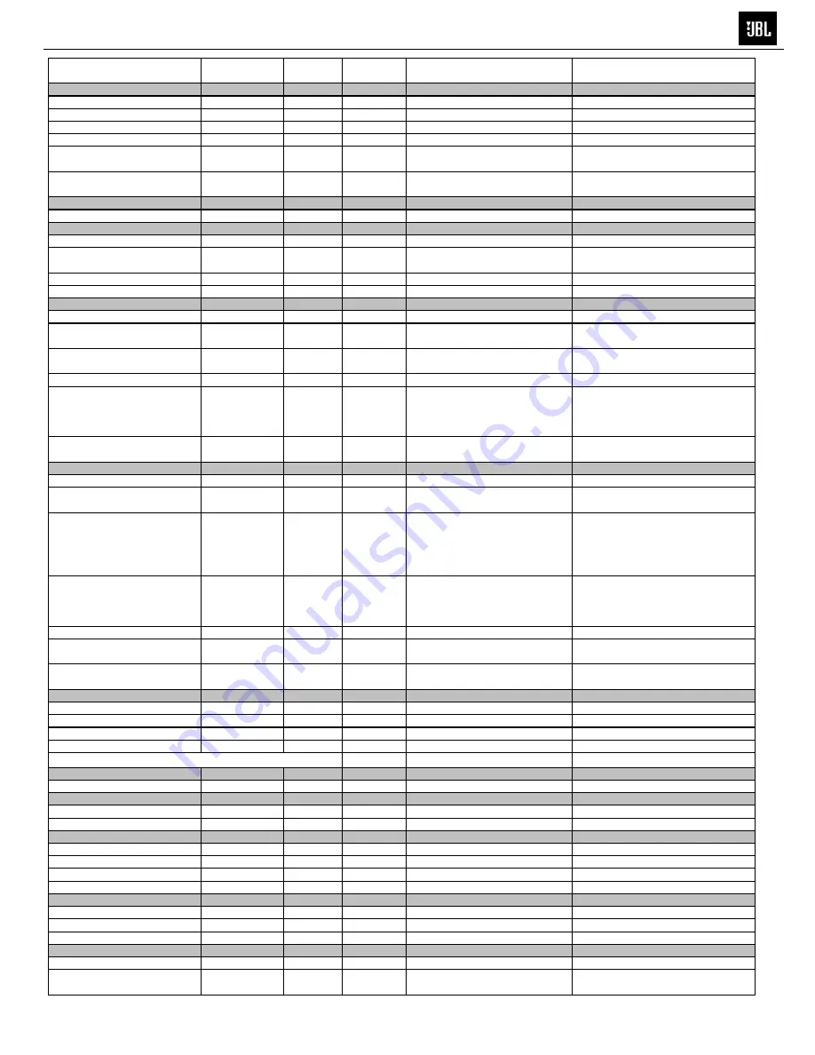
Parameter

Specification

Unit

QA Test 

Limits

Conditions

Notes

Signal Sensing (ATO)

Auto-Turn-On (yes/no)

YES

Functional 

ATO Input test frequency

50

Hz

Functional 

ATO Line level input

1.5

mV

Functional 

Maximum acceptable level.

ATO Turn-on time

5

ms

Functional  Amp connected and AC on, then 

input signal applied

Auto Mute/ Turn-OFF Time

5-15

minutes

5-15

T before muting, after signal is 

removed

Auto turn of time (T)   must be  5 > T < 

15 Minutes

Power on Delay time

3

sec.

4

AC Power Applied

Transients/Pops

ATO Transient

0.5

V-peak

0.5V

@ Speaker Output

Amplifier activated by signal presence 

at the Line input

Turn-on Transient

0.5

V-peak

0.8V

@ Speaker Output

AC Line cycled from OFF to ON

Turn-off Transient

0.5

V-peak

0.8V

@ Speaker Output

AC Line cycled from ON to OFF

Efficiency

Efficiency

65

%

60

Test conducted at rated power 

200W

Nominal Line voltage 

Efficiency at 1/8 of rated power

48

%

45

Test conducted at 25 WRMS

Nominal Line voltage-Rated impedance 

4 Ohms

Standby Input power

15

Watts

16

Nominal Line voltage  RED LED

Idle input power

14

Watts

16

@ nom. line voltage

Maximum allowable  input power under 

nominal  Input voltage and frequency, 

HOT or COLD operation. LED GREEN 

no signal applied

Power Cons. @ rated power

303

Watts

331

@ nom. line voltage

200 Watts @ 4 Ohms nominal line 

voltage

Protections

Short Circuit Protection 

YES

Functional  Direct short at output

Amplifier should resume operation after 

short circuit condition removal 

Thermal Protection 

YES

Functional @1/8 max unclipped Power at 1.06 

times the input voltage

Temperature rise in accessible metal 

parts should not exceed 35K rise for 

domestic version or 30K rise for 

European versions (refer to 

requirements sheet).

DC Offset Protection

YES

-

DC present at Speaker Out leads

Design must insure no Offset/DC 

Voltage at the speaker output  under 

any operating condition including 

abnormal operation

Line Fuse Rating
USA-Domestic 

3.15

Amps

3.15

Type-T or Slo Blo-250 V

Internal fuse with UL/SEMKO rated 

holder

EU

2

Amps

2

Type-T or Slo Blo-250 V, Low 

Breaking capacity

Internal fuse with UL/SEMKO rated 

holder

Mechanical

System weight

39

Lbs

Reference

Subwoofer 

Dimensions (H x W x D)

8 x 13-1/4 x 15-3/8 inches

Reference

Depth includes antenna but no grill

SYSTEM PERFORMANCE USING WIRELESS Tx 

THD @ 1 Watt

0.43

%

0.5

22K filter

Tx Input Impedance

Line Input (LFE)

7.3K

ohms

n/a

Nominal @ 1KHz

System Sensitivity

Using Tx

Input Frequency

50

Hz

50

Nominal Freq.

System level, using Tx

LFE Input

6.4

mVrms

±1dB

To 1 Watt

System level, using Tx

System gain

50

dB

±1dB

To 1 Watt

System level, using Tx

System Signal to Noise

Using Tx

SNR-A-Weighted

75

dBA

70

relative to 1W

A-Weighting filter

SNR-unweighted

57

dBr

55

relative to 1W

22K filter

Filters

System filter

None

Hz

Should not have any effect on the 

FR of the system


 ES150PW 


3

Summary of Contents for ES150PW

Page 1: ...ES Series ES150PW Wireless Powered Subwoofer Service Manual JBL Consumer Products 250 Crossways Park Dr Woodbury New York 11797 Released 2008 Rev1 3 2009 Discontinued XXXX...

Page 2: ...e from 50Hz to 150Hz 24dB octave Frequency Response 27Hz 150Hz Operating Range Up to 75 22m depending upon conditions RF Operating Frequency 2 4GHz Subwoofer Dimensions H x W x D 18 x 13 1 4 x 16 1 8...

Page 3: ...e input driven LFE Mode local Signal to Noise SNR A Weighted 80 dBA 75 relative to 1W A Weighting filter SNR unweighted 65 dBr 60 relative to 1W 22K filter Residual Noise Floor 1 5 mVrms max 2 5 Volum...

Page 4: ...ns Short Circuit Protection YES Functional Direct short at output Amplifier should resume operation after short circuit condition removal Thermal Protection YES Functional 1 8 max unclipped Power at 1...

Page 5: ...e RED LED Tx Idle Power 2 34 Watts Reference 120VAC line voltage Unit in operation Locked to Rx section Solid GRN Tx Idle Power 1 64 Watts Reference 120VAC line voltage Unit in operation NOT locked to...

Page 6: ...000 08392 E Outer Carton ES150PW Beech 1 9 400 000 08388 E Outer Carton ES150PW Black 1 10 Carton Label 1 11 244 100 05276 1BAE Grille w logo packaged 1 12 Accessory box consisting of 1 a Carton 1 b 0...

Page 7: ...t Control Subwoofer Level Volume Control Phase Switch Wireless Antenna Transmitter Transmitter Antenna Transmitter Power Supply Input B Transmitter ID Code Selector Transmitter Sub Input CONTROLS AND...

Page 8: ...tions 1 Connect a subwoofer cable from the subwoofer or LFE output of your receiver to the Sub In C on the transmitter 2 Plug the transmitter module s power supply into the wall outlet and connect the...

Page 9: ...woofer Adjust Level Set the overall volume control of the preamplifier or stereo to a comfortable level Adjust the Subwoofer Level Control until you obtain a pleasing blend of bass Bass response shoul...

Page 10: ...E JBL Logo 1 7 352 KM03520D1148 E Screw LED Plate 4 8 25PR12FZX DW04 E 10 Woofer DCR 3 4 1 9 213 100 05156 0AAE 10 Trim Ring 1 10 352 KM04020D1149 E Screw Trim Ring 8 11 321 ABS 00008 E Foot Plastic m...

Page 11: ...ES150PW 10...

Page 12: ...n top of Subwoofer should be momentarily Green then Orange 7 Turn LEVEL control full clockwise MAX immediate and vigorous bass response should be heard and felt from port tube opening on the bottom 8...

Page 13: ...er and test Driver Function 1 Remove woofer from cabinet detach and wire clips 2 Check DC resistance of woofer it should be 3 4 ohms 10 3 Connect a pair of speaker cables to driver terminals Cables sh...

Page 14: ...ES150PW 13...

Page 15: ...ES150PW 14...

Page 16: ...ES150PW 15...

Page 17: ...ES150PW 16...

Page 18: ...output power noise OK Check pre board power board Vcc 15V ect Test frequency Response OK Check U102 uR133 C121 R135 C122 ect Test input sensitivity OK Check U101 R117 R112 R114 etc Test protection OK...

Page 19: ...no signal out check VD 17VDC Check VA 15VDC Check 12VDC 3 6VDC Check D1 L01 D05 Q04 D0 3 Q03 Q01 Q02 etc OK END Check MD01WH4924 Check Q06 Q05 etc Check Q07 D08 U01 D10 U02etc LED light green or red C...

Page 20: ...leshooting Flow Chart no yes yes yes no yes yes no yes AMP no signal out Check 3 7VDC Check R505 U501 D501 L5 01 L502 U01 etc OK END Check MD01 RX 11G Check LAUNCHER signal Check MD01 LRCK signal Chec...

Page 21: ...ES150PW 20...

Page 22: ...ES150PW 21...

Page 23: ...2 1 3 2 1 3 ES150PW 22...

Page 24: ...ES150PW 23...

Page 25: ...ES150PW 24...

Page 26: ...ES150PW 25...

Page 27: ...ES150PW 26...

Page 28: ...503 e Capacitor 1000P 50V 10 RoHS 1 C165 130 3F104Z503 E Capacitor 0 1U 50V 80 20 RoHS 2 C163 C164 130 CH101J503 E Capacitor 100P 50V 5 RoHS 2 C159 C160 135 3107M16 E Capacitor 100uF 16V 20 RoHS 2 C16...

Page 29: ...0805 1 10W 1 RoHS 1 R128 118 08054301F E SMD Resistor 0 1W 1 4 3K RoHS 1 R254 118 08054421F E SMD Resistor 0 1W 1 4 42K RoHS 2 R205 R207 118 08054701F E SMD Resistor 4 7K 0805 1 RoHS 1 R144 118 080547...

Page 30: ...W 124K 1 MF26mm RoHS 1 R190 116 161271F26 E Resistor1 27K 1 6W 1 MF RoHS 1 R251 116 162051F26 E Resistor 2 05K 1 6W MF 26mm RoHS 1 R252 116 162611F26 E Resistor 1 6W 2 61K 1 26mm RoHS 1 R253 116 16487...

Page 31: ...LIPSBZX84 C12 RoHS 4 Z3 Z4 Z5 Z6 192 233f640n e Transistor IRF640N INTERNATIONAL RoHS 1 Q11 192 232irf9640 e FET IRF9640 IR P CH TO220 RoHS 2 Q10 Q10B Miscellaneous 122 13151k0190 e CHOKE SA 500 280 P...

Page 32: ...630R345B E Fuse holder UL CSA 6 30mm R3 45B RoHS 1 122 14103M4200 E Inductor RT251510 103N 10mH RoHS 1 L02 122 14501M0650 E Inductor 0 5mH 0 65 RoHS 1 L01 130 3F102MB50 E Capacitor Y1 1NF 20 250V RoH...

Page 33: ...04012D024 E 4 12WOOD SCREW BLK RoHS 4 351 AM02606A011 E M2 6 6 Machine screw cross BLK RoHS 2 351 AM03008A078 E M3 8 MACHINE SCREW CROSS WITH NICKEL RoHS 10 351 AM03008A079 E M3 8 MACHINE SCREWCROSS B...

Page 34: ...include Ther mal Shutdown VCC under voltage lockout Gate drive under voltage lockout and Max Duty Cycle limiter Features n Integrated 100V N Channel buck switch n Internal VCC regulator n No loop com...

Page 35: ...arator The regulation threshold is 2 5V 6 RON SD On time set pin Ton 1 25 x 10 10 RON VIN A resistor between this pin and VIN sets the switch on time as a function of VIN The minimum recommended on ti...

Page 36: ...one input to be used as an active LOW clock enable CE input The pin assignment for the CP and CE inputs is arbitrary and can be reversed for layout convenience The LOW to HIGH transition of input CE...

Page 37: ...input active LOW 7 Q7 complementary output from the last stage 9 Q7 serial output from the last stage 2 CP clock input LOW to HIGH edge triggered 8 GND ground 0 V 10 Ds serial data input 11 12 13 14 3...

Page 38: ...to the LOW to HIGH clock transition q lower case letters indicate the state of the referenced output one set up time prior to the LOW to HIGH clock transition X don t care LOW to HIGH clock transition...

Page 39: ...including digital interpolation fourth order delta sigma digital to analog conversion digital de emphasis and switched capacitor analog filtering The advantages of this architecture include ideal dif...

Page 40: ...sed to gain access to extra de emphasis modes Internal Serial Clock Mode In the Internal Serial Clock Mode the serial clock is internally derived and synchronous with the master clock and left right c...

Page 41: ...put STM810 812 140ms RESET PULSE WIDTH MIN LOW SUPPLY CURRENT 6 A TYP GUARANTEED RST RST ASSERTION DOWN TO VCC 1 0V OPERATING TEMPERATURE 40 C to 85 C Industrial Grade LEAD FREE SMALL SOT23 and SOT143...

Page 42: ...Figure 2 Logic Diagram STM809 810 Note 1 For STM810 Figure 3 Logic Diagram STM811 812 Note 1 For STM812 Table 2 Signal Names Note 1 STM810 812 only 2 STM811 812 only Figure 4 SOT23 3 Connections Figu...

Page 43: ...ace with any SPI supporting device I2 S left or right justified including ADCs DACs digital audio streams such as S P DIF or USB A development kit is required to modify the DASI port and or to modify...

Page 44: ...C7 General Purpose IO port PC7 13 PC6 PC6 PC6 General Purpose IO port PC6 14 PC5 PC5 PC5 General Purpose IO port PC5 15 PC4 PC4 PC4 General Purpose IO port PC4 16 PC0 MCLK PC0 MCLK General Purpose IO...

Page 45: ...omization can be performed at the time of production or during product assembly The following two diagrams and two tables describe how to configure the WHAM2 for different operations by changing jumpe...

Page 46: ...t or output Edge pin 18 J7 DNP J8 0R Pin 18 is AN1 XInC2 muxed analog input 1 Input voltage range of ADC is 0V to 1 8V J9 0R J10 DNP Pin 19 is FW selectable as either GPIO port pin PI1 or baseband uni...

Page 47: ...ES150PW 46...

Page 48: ...10 9 8 TL074 U106 C 5 6 7 TL074 U106 B 3 2 1 TL074 U106 A P106 VEE U106 F VDD U106 E 12 13 14 TL074 U106 D ES150PW 47...

Page 49: ...2 3 1 TL072 U105 A VEE U105 D VDD U105 C 6 5 7 U105 B TL072 ES150PW 48...

Page 50: ...Green Red D401 LED_5DIA ES150PW 49...

Page 51: ...ES150PW 50...

Page 52: ...ES150PW 51...

Page 53: ...ES150PW 52...

Page 54: ...ES150PW 53...

Page 55: ...502 C501 47u 100V 100n C104 R503 120R 1 R504 240R 1 C508 470u P501 R505 10R 1 4W MO 103 C505 LM5008 U501 470u C506 L501 220u C507 1 R501 330K R502 270K 2 1 D501 10BQ100 22u L502 C503 1 100V ES150PW 54...

Page 56: ...L01 56R 2 1 ES150PW 55...

Page 57: ...C322 104z VEE U109 D VDD U109 C 220R R333 220R R332 JK1 C332 100P 5K1 R321 100P C318 R330 10K C320 104z 100R R315 5K1 R318 5K1 R322 2 3 1 TL 072 U109 A 5K1 R316 100P C319 22u C312 5K1 R317 5K1 R319 6K...

Page 58: ...L 072 U103 B VEE U102 F VEE U103 D 5 6 7 TL074 U102 B 3 2 1 TL074 U102 A 2 3 1 TL 072 U108 A VDD U101 C VEE U108 D VDD U102 E 12 13 14 TL074 U102 D 2 3 1 U101 A TL 072 6 5 7 TL 072 U108 B VDD U103 C 2...

Page 59: ...ES150PW 58...

Reviews: