background image


©On-Bright Electronics                                                                                                                        

Confidential


- 11 -                                                            

   OB_DOC_DS_69CC1 


OB2269C

Current Mode PWM Controller

Frequency Shuffling

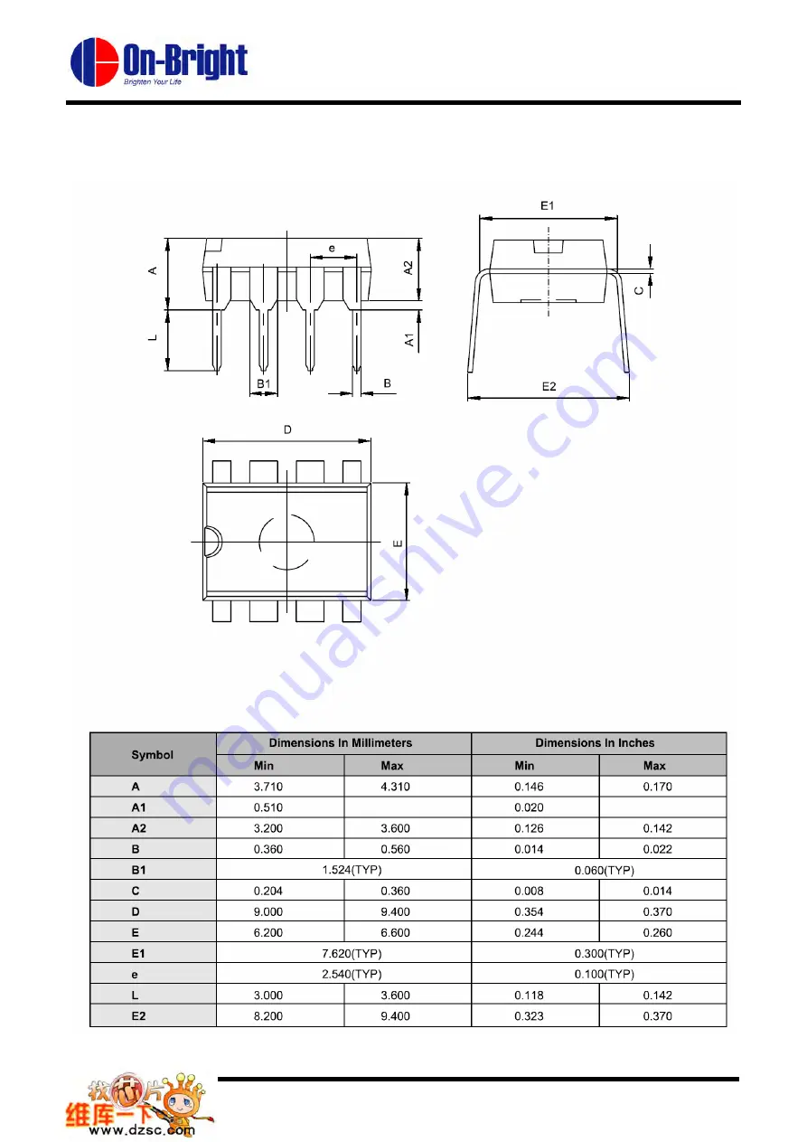
PACKAGE MECHANICAL DATA 

8-Pin Plastic DIP 


On-Bright Confidential to Lycon (志恒通电子)

JBL

150P / 230V Service Manual

Page 38 of 50

Summary of Contents for SP-150

Page 1: ...mer Group Inc Rev 0 02 2012 8500 Balboa Boulevard Northridge California 91329 OWNER S MANUAL 2 SPECIFICATIONS 7 PACKAGE GUIDE AND PARTS 8 EXPLODED VIEW 9 TROUBLESHOOTING FLOW CHART 11 PARTS LIST 12 SEMICONDUCTOR PINOUTS 18 PCB DRAWINGS 41 BLOCK DIAGRAMS 47 SCHEMATIC DIAGRAMS 49 CONTENTS ...

Page 2: ...f the SP 150 is also simple to connect and set up We re confident that this JBL subwoofer will provide every note of enjoyment that you expect and that when you think about purchasing additional audio equipment for your home car or office you will once again choose JBL products This quick start guide contains all the information you need to set up connect and adjust your new subwoofer For more in ...

Page 3: ...paratus when the appa ratus has been exposed to rain or moisture when the apparatus does not operate normally or the apparatus has been dropped 15 Do not expose this apparatus to dripping or splashing and ensure that no objects filled with liquids such as vases are placed on the apparatus 16 To completely disconnect this apparatus from the AC mains discon nect the power supply cord plug from the A...

Page 4: ...mplifiers have corresponding positive and negative and connectors The SP150 Speaker Level Input connectors are marked and beneath the connector levels Additionally the connectors have red markings while the connectors have black markings To ensure proper polarity connect each connector on the back of your receiver or amplifier to the respective red connector on each speaker Connect the connectors ...

Page 5: ...ing positions may yield very good results while others may have far too much or too little bass at certain frequencies In many rooms placing the subwoofer along the same plane as the left and right speak ers 2 can produce the best integration between the sound of the subwoofer and that of the left and right speakers In some rooms the best performance could even result from placing the subwoofer be...

Page 6: ... LINE LEVEL SUBWOOFER OUTPUT FRONT SPEAKERS SURROUND SPEAKERS CENTER SPEAKER SP150 Subwoofer Front Left Speaker Speaker Wire not supplied Speaker Wire not supplied Receiver or Amplifier Front Right Speaker JBL 150P 230V Service Manual Page 5 of 50 ...

Page 7: ... its bass output while placing it away from any walls or corners will tend to lessen its bass output Subwoofer Adjustments Phase The Phase switch determines whether the subwoofer driver s piston like action moves in and out in phase with the satellite speakers If the subwoofer were to play out of phase with the satellite speakers the sound waves from the satellites could partially cancel out the w...

Page 8: ... 230V Service Manual Page 7 of 50 This place with CUT is to fit front of subwoofer packing illustration sub PE bag EPE bag styrofoam top cover manual styrofoam bottom cover desiccant 25g bag carton sealing tape ...

Page 9: ...4 JBL 150P 230V Service Manual Page 8 of 50 exploded view No P N Name Q ty Q ty Name P N No port tube paper tube tube head cabinet self tapping screw SP150 230 AMP self tapping screw lighted badge woofer foot ...

Page 10: ...0020034 3自攻螺丝 5 13 70010031 机牙螺丝M3 8 8 14 10080121 散热片30 15 13 2mm 1 15 70010051 机牙螺丝M3 18 1 16 70010043 带平垫机牙螺丝M3 12 2 17 70070002 外六角螺母带平垫弹垫 1 1R 序号 料号 料号 名称 名称 用量 用量 JBL 150P 230V Service Manual Page 9 of 50 Part No Part Name Q ty No Part No Part Name Q ty AL panel filter pcb poweramp pcb M screw with flat washer M3 6 M screw spacer S5 10mm M3 steel bracket EVA piece fuse holder cord strain rel...

Page 11: ...arts related to them emphasis is to check if U2 is defective emphasis is to check if is Q1 C3 D5 D6 D7 defective and check if R26 R25 C57 C54 is defective NO Test Sensitivity OK check U6 A and parts related to it check 12V voltage 1V NO NO check VCC voltage Test limiter circuit OK check if U2 is defective test method pls refer to above items check limiter circuit emphasis is to check if U2 C64 C65...

Page 12: ...L 34 50050029 SMT Cap 1 C27 2 C265 53 1 C10 50050022 SMT Cap 50050012 SMT Cap 50050067 SMT Cap 7 C4 6 19 22 1W 22Ω 5 2512 1W 100K 5 2512 104 50V 10 0805 X7R 102 50V 10 0805 X7R 11170615 SMT Res 1 R13 2 R14 15 1 R23 11170520 SMT Res 11170599 SMT Res 11170515 SMT Res 2 R32 33 1 4W 1M 1 1206 1 4W 2M 1 1206 0 75W 10Ω 5 2010 1W 0 1Ω 1 2512 11170487 SMT Res 1 R2 3 R17 19 20 2 R1 16 11170485 SMT Res 1117...

Page 13: ...e pin Ф1 7mm 14010167 MOS 1 L1 1 T1 1 Q1 24060130 inductor 24060123 common mode inductor 13030099 hi FREQ transformer 2 L3 6 Φ3 5 9mm vertical P 5mm L 4mm 16 19 22uH L 4mm 22uH 3A Φ8 10mm P 5mm L 4mm L EE25 12mH diameter 0 6mm 24060129 inductor 2 L2 4 2 L8 9 2 L5 7 17010240 E C 24060006 color code inductor 24060052 bead 1 C1 220uF 35V 105 20 Φ8 12mm L 4mm 1000uF 35V 105 20 Φ13 21mm L 4mm 120uF 400...

Page 14: ...egree 1 CON2B 1 CON1A 1 1 8W 0Ω 1 0805 1 17020015 E C 17010073 E C 1 C71 6 C36 38 41 43 2SA1015GR PNP TO 92 L 4mm 10uF 50V 105 20 Φ4 7mm L 4mm 22uF 25V 105 20 Φ4 7mm L 4mm 220uF 25V 105 20 Φ6 3 12mm L 4mm 17020056 E C 1 Q6 1 Q21 1 C70 14040205 SMT IC 14010001 Transistor 14010002 Transistor 1 U2 MMBT3904LT1 1AM SOT23 NPN MOTOROLA MMBT3906LT1 2A SOT23 PNP MOTOROLA TDA8920CTH HSOP24 NXP 2SC1815GR NPN...

Page 15: ...Z1 2 18070037 SMT Diode 104 50V 10 0805 X7R 1 2W IN4148 LL 34 50050022 SMT Cap 102 50V 10 0805 X7R 1 C40 18070001 SMT Diode 2 C33 CP 5 C12 14 37 200 50050012 50050038 SMT Cap 101 50V 5 0805 NPO 2 C6 23 221 50V 5 0805 NPO 50050010 SMT Cap 11170622 SMT Res R03 04 11170406 SMT Res 1W 680Ω 5 2512 2 R01 02 2 11170376 SMT Res 1 4W 3K 1 1206 1 R72 11170628 SMT Res 1W 200Ω 5 2512 11170138 SMT Res 11170139...

Page 16: ...hing 30 15 13 2mm nature AL 1 1 1 10100204 AL panel Φ0 6 28mm 1 connect shielding plate to GND of preamp pcb 220 190 3 0mm black painting 11080024 Jumper Wire 30060109 EVA piece 10010102 PCB S100ETH 5 copper foil at one side 55 55 1mm 1 1 70010021 M Screw with flat washer M3 6mm colorful 1 CON2 10250022 steel bracket 55 55 3mm double side adhensive 40190007 RCA connector 16050052 7P shielding cabl...

Page 17: ...n spring terminal 2 30060099 EVA piece 145 27 11 5mm adhensive at both sides 2 11080041 Jumper Wire 220uF 50V 105 20 Φ13 21mm L 10mm 10010049 PCB 40200001 spring terminal Φ0 8 17 5mm L 4mm 1 paste on spring terminal 1 solder on spring terminal 1 solder spring terminal 15 13 5 5mm adhensive at both sides UL1617 18 L 100 10 5mm red XJPCB 146 25 1 6mm 94V0 single side WP4 19B vertical 16130158 cable ...

Page 18: ... BVCEO 50V Collector Current up to 150mA High hFE Linearity Complement to UTC 2SC1815 Lead free 2SA1015L Halogen free 2SA1015G ORDERING INFORMATION Ordering Number Pin Assignment Normal Lead Free Plating Halogen Free Package 1 2 3 Packing 2SA1015 x T92 B 2SA1015L x T92 B 2SA1015G x T92 B TO 92 E C B Tape Box 2SA1015 x T92 K 2SA1015L x T92 K 2SA1015G x T92 K TO 92 E C B Bulk JBL 150P 230V Service M...

Page 19: ...ACTERISTICS Ta 25 C unless otherwise specified PARAMETER SYMBOL TEST CONDITIONS MIN TYP MAX UNIT Collector Base Breakdown Voltage BVCBO IC 100μA IE 0 50 V Collector Emitter Breakdown Voltage BVCEO IC 10mA IB 0 50 V Emitter Base Breakdown Voltage BVEBO IE 10μA IC 0 5 V Collector Cut off Current ICBO VCB 50V IE 0 100 nA Emitter Cut off Current IEBO VEB 5V IC 0 100 nA hFE1 VCE 6V IC 2mA 120 700 DC Cu...

Page 20: ...ure range Tstg 55 125 C Electrical Characteristics Ta 25 C Characteristics Symbol Test Condition Min Typ Max Unit Gate cut off current IGSS VGS 25 V VDS 0 1 0 nA Gate drain breakdown voltage V BR GDS VDS 0 IG 100 mA 25 V Drain current IDSS Note VDS 10 V VGS 0 2 6 20 mA Gate source cut off voltage VGS OFF VDS 10 V ID 0 1 mA 0 15 2 0 V Forward transfer admittance ïYfsï VDS 10 V VGS 0 f 1 kHz 8 22 mS...

Page 21: ...FEATURES Collector Emitter voltage BVCEO 50V Collector current up to 150mA High hFE linearity Complimentary to UTC 2SA1015 ORDERING INFORMATION Ordering Number Pin Assignment Normal Lead Free Halogen Free Package 1 2 3 Packing 2SC1815 x T92 B 2SC1815L x T92 B 2SC1815G x T92 B TO 92 E C B Tape Box 2SC1815 x T92 K 2SC1815L x T92 K 2SC1815G x T92 K TO 92 E C B Bulk JBL 150P 230V Service Manual Page 2...

Page 22: ...e stress ratings only and functional device operation is not implied ELECTRICAL CHARACTERISTICS Ta 25 unless otherwise specified PARAMETER SYMBOL TEST CONDITIONS MIN TYP MAX UNIT Collector Cut off Current ICBO VCB 60V IE 0 100 nA Emitter Cut off Current IEBO VEB 5V IC 0 100 nA Collector Emitter Saturation Voltage VCE SAT IC 100mA IB 10mA 0 1 0 25 V Base Emitter Saturation Voltage VBE SAT IC 100mA ...

Page 23: ...JBL 150P 230V Service Manual Page 22 of 50 ...

Page 24: ...STICS TA 25 C unless otherwise noted Characteristic Symbol Min Max Unit OFF CHARACTERISTICS Collector Emitter Breakdown Voltage 3 IC 1 0 mAdc IB 0 V BR CEO 40 Vdc Collector Base Breakdown Voltage IC 10 mAdc IE 0 V BR CBO 60 Vdc Emitter Base Breakdown Voltage IE 10 mAdc IC 0 V BR EBO 6 0 Vdc Base Cutoff Current VCE 30 Vdc VEB 3 0 Vdc IBL 50 nAdc Collector Cutoff Current VCE 30 Vdc VEB 3 0 Vdc ICEX ...

Page 25: ...a does not convey any license under its patent rights nor the rights of others Motorola products are not designed intended or authorized for use as components in systems intended for surgical implant into the body or other applications intended to support or sustain life or for any other application in which the failure of the Motorola product could create a situation where personal injury or deat...

Page 26: ... CHARACTERISTICS TA 25 C unless otherwise noted Characteristic Symbol Min Max Unit OFF CHARACTERISTICS Collector Emitter Breakdown Voltage 3 IC 1 0 mAdc IB 0 V BR CEO 40 Vdc Collector Base Breakdown Voltage IC 10 mAdc IE 0 V BR CBO 40 Vdc Emitter Base Breakdown Voltage IE 10 mAdc IC 0 V BR EBO 5 0 Vdc Base Cutoff Current VCE 30 Vdc VEB 3 0 Vdc IBL 50 nAdc Collector Cutoff Current VCE 30 Vdc VEB 3 ...

Page 27: ...40 C 0 0350 0 0440 0 89 1 11 D 0 0150 0 0200 0 37 0 50 G 0 0701 0 0807 1 78 2 04 H 0 0005 0 0040 0 013 0 100 J 0 0034 0 0070 0 085 0 177 K 0 0180 0 0236 0 45 0 60 L 0 0350 0 0401 0 89 1 02 S 0 0830 0 0984 2 10 2 50 V 0 0177 0 0236 0 45 0 60 NOTES 1 DIMENSIONING AND TOLERANCING PER ANSI Y14 5M 1982 2 CONTROLLING DIMENSION INCH 3 MAXIMUM LEAD THICKNESS INCLUDES LEAD FINISH THICKNESS MINIMUM LEAD THI...

Page 28: ...JBL 150P 230V Service Manual Page 27 of 50 ...

Page 29: ...JBL 150P 230V Service Manual Page 28 of 50 ...

Page 30: ...at typical applications u SE 2 110 W RL 4 Ω VP 30 V u SE 2 125 W RL 4 Ω VP 32 V u SE 2 120 W RL 3 Ω VP 29 V u BTL 1 210 W RL 8 Ω VP 30 V n Low noise in BTL operation due to BD modulation n Smooth pop noise free start up and switch off n Zero dead time Pulse Width Modulation PWM output switching n Fixed frequency n Internal or external clock switching frequency n High efficiency n Low quiescent cur...

Page 31: ...ion supply voltage Non Operating mode VDD VSS 65 70 V Iq tot total quiescent current Operating mode no load no filter no RC snubber network connected 50 75 mA Stereo single ended configuration Po output power L 22 µH C 680 nF Tj 85 C THD 10 RL 4 Ω VP 30 V 2 110 W THD 10 RL 4 Ω VP 27 V 80 W Mono bridge tied load configuration Po output power L 22 µH C 680 nF Tj 85 C THD 10 RL 8 Ω VP 30 V 2 210 W Ta...

Page 32: ...DA8920CJ TDA8920CTH VSSD VSSA VDDP2 SGND BOOT2 VDDA OUT2 IN2M VSSP2 IN2P n c MODE STABI OSC VSSP1 IN1P OUT1 IN1M BOOT1 n c VDDP1 n c PROT n c 001aai853 24 23 22 21 20 19 18 17 16 15 14 13 11 12 9 10 7 8 5 6 3 4 1 2 TDA8920CJ OSC IN1P IN1M n c n c n c PROT VDDP1 BOOT1 OUT1 VSSP1 STABI VSSP2 OUT2 BOOT2 VDDP2 VSSD VSSA SGND VDDA IN2M IN2P MODE 001aai854 1 2 3 4 5 6 7 8 9 10 11 12 13 14 15 16 17 18 19...

Page 33: ...ymbol Pin Description TDA8920CTH TDA8920CJ VSSA 1 18 negative analog supply voltage SGND 2 19 signal ground VDDA 3 20 positive analog supply voltage IN2M 4 21 channel 2 negative audio input IN2P 5 22 channel 2 positive audio input MODE 6 23 mode selection input Standby Mute or Operating mode OSC 7 1 oscillator frequency adjustment or tracking input IN1P 8 2 channel 1 positive audio input IN1M 9 3 ...

Page 34: ...ic or metal protrusions of 0 25 mm maximum per side are not included SOT411 1 98 02 20 02 04 24 0 5 10 mm scale D L L1 L2 E2 E c A4 A5 A2 m L3 E1 Q w M bp 1 d Z e 2 e e 1 23 j DBS23P plastic DIL bent SIL power package 23 leads straight lead length 3 2 mm SOT411 1 v M D x h Eh non concave view B mounting base side B β e1 bp c D 1 E 1 Z 1 d e Dh L L3 m 0 75 0 60 0 55 0 35 30 4 29 9 28 0 27 5 12 2 54...

Page 35: ...ons Notes 1 Limits per individual lead 2 Plastic or metal protrusions of 0 25 mm maximum per side are not included SOT566 3 0 5 10 mm scale HSOP24 plastic heatsink small outline package 24 leads low stand off height SOT566 3 A max detail X A2 3 5 3 2 D2 1 1 0 9 HE 14 5 13 9 Lp 1 1 0 8 Q 1 7 1 5 2 7 2 2 v 0 25 w 0 25 y Z 8 0 θ 0 07 x 0 03 D1 13 0 12 6 E1 6 2 5 8 E2 2 9 2 5 bp c 0 32 0 23 e 1 D 2 16...

Page 36: ...perature Coefficient 50PPM Temperature Compensated For Operation Over ORDERING INFORMATION Full Rate Operating Temperature Range Adjustable Output Voltage TL431 Fast Turn on Response TL431 A Sink Current Capability 1 to 100 TL431 C Low 0 2 Typ Dynamic Output Impedance TL431F Low Output Noise TL431 AF TL431 CF FUNCTION BLOCK DIAGRAM HTC TL431 TL431 A TL431 C 4N SOT 89 TO 92 Package Device 4A 4C Mar...

Page 37: ...lamp Continuous Current 10 mA VFB Input Voltage 0 3 to 7V VSENSE Input Voltage to Sense Pin 0 3 to 7V VRT Input Voltage to RT Pin 0 3 to 7V VRI Input Voltage to RI Pin 0 3 to 7V Min Max Operating Junction Temperature TJ 20 to 150 o C Min Max Storage Temperature Tstg 55 to 150 o C Lead Temperature Soldering 10secs 260 o C Note VDD_Clamp has a nominal value of 35V Stresses beyond those listed under ...

Page 38: ...large value resistor to rectified line input for Startup IC supply and line voltage sensing 4 RI I Internal Oscillator frequency setting pin A resistor connected between RI and GND sets the PWM frequency 5 RT I Temperature sensing input pin Connected through a NTC resistor to GND 6 SENSE I Current sense input pin Connected to MOSFET current sensing resistor node 7 VDD P DC power supply pin 8 GATE ...

Page 39: ...dential 11 OB_DOC_DS_69CC1 OB2269C Current Mode PWM ControllerFrequency Shuffling PACKAGE MECHANICAL DATA 8 Pin Plastic DIP O n B r i g h t C o n f i d e n t i a l t o L y c o n 志 恒 通 电 子 JBL 150P 230V Service Manual Page 38 of 50 ...

Page 40: ...ronics Confidential 12 OB_DOC_DS_69CC1 OB2269C Current Mode PWM ControllerFrequency Shuffling 8 Pin Plastic SOP O n B r i g h t C o n f i d e n t i a l t o L y c o n 志 恒 通 电 子 JBL 150P 230V Service Manual Page 39 of 50 ...

Page 41: ...JBL 150P 230V Service Manual Page 40 of 50 ...

Page 42: ...JBL 150P 230V Service Manual Page 41 of 50 ...

Page 43: ...JBL 150P 230V Service Manual Page 42 of 50 ...

Page 44: ...JBL 150P 230V Service Manual Page 43 of 50 ...

Page 45: ...JBL 150P 230V Service Manual Page 44 of 50 ...

Page 46: ...JBL 150P 230V Service Manual Page 45 of 50 ...

Page 47: ...JBL 150P 230V Service Manual Page 46 of 50 ...

Page 48: ...JBL 150P 230V Service Manual Page 47 of 50 ...
Page 49: ...74 220K R75 2 2K D6 1N4148 D7 1N4148 C35 47 25 C34 22 50 R68 1K R76 5 1K C36 22 50 R78 2K R1 3K R77 15K 3 2 1 U7 A NJM4558 C39 22 50 8 4 U6 C NJM4558 8 4 U7 C NJM4558 C9 100 25 C6 CC101 C8 1 50 R20 300K R19 1K R21 100K D3 1N4148 R25 2M R27 10K R30 3K 1206 D2 1N4148 R17 120K C18 C37 104 cc R18 2 7K VR1 A A50K VR1 B A50K S3 LED R87 NC R86 NC C40 CC221 1 2 3 VR2 A C50K 4 5 6 VR2 B C50K 7 8 9 VR2 C C5...

Page 50: ...471 50V C34 471 50V Q6 2SC1815 Q21 2SA1015 Z1 10V R80 6 8k Z3 10V R81 6 8k R82 825 1206 R83 1 54K 1206 Z4 nc Z5 NC Q22 MMBT3906LT1 Q23 MMBT3906LT1 R84 20K R85 20K C36 22 25V C37 22 25V C38 22 25V C41 22 25V C42 22 25V C43 22 25V C44 104 50 C45 104 50 C46 104 50 C47 104 50 C8 0 47u 50V C23 0 47u 50V 1 2 3 4 5 6 7 8 CON1A 1 2 3 4 5 6 CON2B C24 471 50V 1 2 3 4 5 6 CON2A 1 2 3 4 5 6 7 8 CON1B L5 22UH ...

Page 51: ...X3 X2 224 CY1 471 400V Y1 CY2 471 400V Y1 L1 12mH CX1 X2 224 R1 2M 1206 CY3 222 400V Y1 C10 105 25v 1 2 3 4 U1 PC817 R24 1K R7 220 R8 7 5K C6 104 50 C7 NC R9 2 7K R10 18K R11 3 6K U5 TL431 D6 F12C20C D5 F12C20C T1 L2 100UH L4 100UH C12 220 35V C16 220 35V C17 100 35V C18 100 35V C19 104 50 C20 104 50 C21 104 50 C5 104 50 C4 104 50 C22 104 50 C2 1000 35V C13 1000 35V R3 NC R6 NC C11 1000 35V C14 10...

Reviews: