(No.MB160)1-31
SECTION 4
ADJUSTMENT
4.1
Alignment and adjustment
4.1.1 Tuner
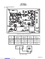
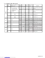
* Adjustment Location of Tuner board
Fig.1 OSC Voltage
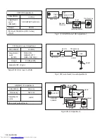
AM(MW) OSC
Adjustment
Output
1~7.0±0.5V
Received FREQ.
Adjustment
point
522~1611 kHz
MO
AM(MW) RF
Adjustment
ITEM
594 kHz
MA
Maximum
Output (Fig.1)
LW OSC
Adjustment
146~290 kHz
LO
2~7.0±0.5V
LW RF
Adjustment
150 kHz
LA
Maximum
Output (Fig.1)
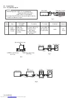
Main
board
VT
GND
TESTER
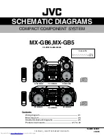
Summary of Contents for CA-MXGB5
Page 45: ... M E M O ...
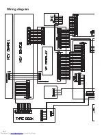
Page 46: ...2 1 Wiring diagram ...
Page 47: ...2 2 ...
Page 50: ...2 5 Standard schematic diagrams Main section MX GB6 ...
Page 53: ...2 8 safety assurance parts placing those parts make se the specified one ...
Page 54: ...2 9 Main section MX GB5 ...
Page 58: ...2 13 FL Key control section common ...
Page 59: ...2 14 ...
Page 60: ...2 15 CD section common ...
Page 61: ...2 16 ...
Page 62: ...2 17 Printed circuit boards Main board ...
Page 63: ...2 18 Amp board ...
Page 64: ...2 19 Front board ...
Page 65: ...2 20 CD board ...

