background image

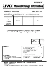
MB-MCI-00057 (1/6)

SUBJECT :


Addition of part

Date : 14.

 Feb. 2005

The following parts have been changed. Please note these new parts in your service manual.
We suggest that you order the parts concerned as apares.
Parts identified by the        symbol are critical for safety. Replace only with specified part numbers.

 Model & Manual No.

MX-KA7

JW

(No.MB039)

 Location

   Parts list

 Reference Information

------

 Performed at factory

#1~

CD-ROM No.

SML200311V11

 A. To improve performance.          E.  Standardization of part.

  B.  To improve reliability.

F.  For your demand.

  C. To improve safety.

G. Correction of misprint.

  D. To improductivity

H. Others.

 A.  Completely interchangeable.
 B.  Previous part can be used for new set,but new

       part can not be used for previous set.

 C.  New part can be used for previous set,but
       previous part can not be used for new set.
 D.  Not interchangeable.
 E.  Addition
 F.  Deletion

COMMENTS :

FOB

(New Parts)

Itg

Rsn Note

E        H

----

ATTACHMENT

(  ) NONE  (  ) COMPONENT / PWBLAYOUT

  (  ) SCHEMATIC  DIAGRAM   (  ) ADJUSTMENT PROCEDURE

(  ) EXPLODED VIEW

INTERCHANGEABILITY

REASON FOR CHANGE

VICTOR COMPANY OF JAPAN,LTD, 


AV & Multimedia Company


1-10-1,Ohwatari-chou. Maebashi-shi,Gunma-ken.371-8543, Japan    Facsimile : 81-27-254-8977  Telephone : 81-27-254-8952

AV Group. 15300

Global Quality Management Dept.

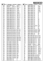
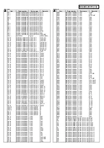
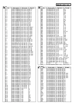
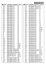
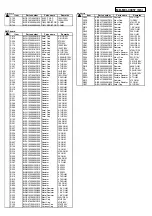
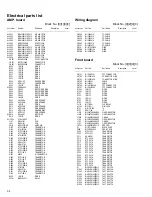
Some parts numbers are missing on Service Manual No.MB039.
Please utilize the following parts list together with original one.

Summary of Contents for CA-MXKA7

Page 1: ...nt for laser products 1 4 Disassembly method 1 5 Adjustment method 1 18 Flow of functional operation until TOC read 1 20 Maintenance of laser pickup 1 21 Replacement of laser pickup 1 21 Description of major ICs 1 22 CA MXKA7 SP MXKA7 SP MXKA7 Area Suffix JW Mexico Panama SERVICE MANUAL COMPACT COMPONENT SYSTEM MX KA7 Wiring connection 1 33 ...

Page 2: ...uired the original lead routing and dress should be observed and it should be confirmed that they have been returned to normal after re assembling 5 Leakage currnet check Electrical shock hazard testing After re assembling the product always perform an isolation check on the exposed metal parts of the product antenna terminals knobs metal cabinet screw heads headphone jack control shafts etc to be...

Page 3: ...er diode in the optical pickup The testers internal power source can easily destroy the laser diode 4 Handling the CD changer unit optical pickup 1 Do not subject the CD changer unit optical pickup to strong shocks as it is a sensitive complex unit 2 Cut off the shorted part of the flexible cable using nippers etc after replacing the optical pickup For specific details refer to the replacement pro...

Page 4: ...ation when the drawer is open and the safety interlocks have failed or are defeated It is dangerous to defeat the safety switches Important for laser products FUSE CAUTION CAUTION REPLACE WITH SAME TYPE AND RATING FUSE S ATTENTION REMPLACER PAR UN LES FUSIBLE S DE MEME TYPE ET DE MEME VALEUR 5 CAUTION If safety switches malfunction the laser is able to function 6 CAUTION Use of controls adjustment...

Page 5: ... loading motor and belt of the CD changer tray Replacing the CD tray rotor belt of CD changer and removing the motor Front panel assembly Removing the cassette deck mechanism Removing the earphone jack PCB Removing the control FL PCB Removing the switch PCB and ACTIVE BASS EX switch PCB Removing the cassette deck main motor and replacing the main belts Removing the leaf switches of the cassette de...

Page 6: ...sure to use fuses with the specified ratings Replacing the heat sink cover See Fig 3 1 Remove four screws B from the rear panel 2 Pull the heat sink cover outward Fig 1 Fuse F951 3 15A 250V Fuse F952 1 6A 250V Replacing the power IC See Fig 2 Prior to performing the following procedure remove the top cover 1 Remove the two screws A from the heat sink between the power IC 2 Remove the solder fixing...

Page 7: ...ain the top cover from the panel rear of the body 2 Remove six screws D that retain the top cover from the two sides of the body 3 Remove the top cover from the body by lifting it toward the rear Fig 5 Fig 4 Right Front panel assembly D D Left Front panel assembly D D Top cover C C ...

Page 8: ...ent damage a From the front panel side of this set push in the sections marked with arrows and pull out the CD tray toward the front b Remove the CD tray panel by pushing both of its extremities upward in the direction of the arrows c Push the CD tray deep into the set 1 Disconnect the cord wires from the CD PCB CN703 and CN203 2 From the rear of the set remove two screws E three screws F and four...

Page 9: ...1 on the power amp PCB 2 Remove one screws H retaining the front panel assembly onto the bottom of the body 3 Remove two screws I on the left and right side of the set retaining the panel front from the bottom and then remove then GND lug b that comes from the power amp and supply PCB 4 Disengage the claws c on both sides of the front panel assembly and then remove the assembly Fig 10 H Fig 11 I e...

Page 10: ...03B and CN604 on the CD PCB which is located on the back side of the CD changer unit 2 The four screws J that retain the CD PCB should be removed 3 Remove the CD PCB by pulling it toward the side where the CN601 is located 4 Using solder short the CD pickup to connect to short round Caution After re connecting the wires be sure to remove the shorting solder from the GND connection 5 Disconnect the...

Page 11: ...cedures remove the top cover Also remove the CD changer unit 1 Turn the CD changer mechanism cover base and remove the screws d connecting the unit to the CD changer mechanism assembly 2 Removing four screws e retaining the CD mechanism holder assembly Caution When replacing the CD changer mechanism assembly be sure not to mistake the positions of the silver color and copper color spring CD change...

Page 12: ...over Also open the CD changer tray 1 Remove the two screws L retaining the CD changer tray loading motor 2 Remove the two screws M retaining the gear plate and take it out after remove the rotor belt from the pulley Replacing the CD turn table and remov ing the motor See Fig 19 Prior to performing the following procedures remove the top cover Also remove the CD changer unit 1 Remove the one screws...

Page 13: ...rews Z retaining the cassette deck mechanism Removing the earphone jack PCB See Fig 20 Prior to performing the following procedures remove the top cover Also remove the CD changer unit Also remove the front panel assembly 1 Remove the screw with the washer P that retains the earphone jack PCB Removing the control FL PCB See Fig 21 Prior to performing the following procedures remove the top cover A...

Page 14: ...el assembly 1 Pull out the volume control knob from the front of the front panel assembly Fig 22 2 Remove six screws Q retaining the front panel assembly Fig 21 3 Remove the control FL PCB 4 Remove eleven screws R retaining the switch key 1 PCB Fig 20 5 Remove two screws S retaining the sound mode and CD function key 2 switch PCB Fig 21 Fig 22 Fig 23 Volume knob Front panel assembly Volume shaft F...

Page 15: ...ches 5 Pull out the leaf switches from the front side of the cassette deck mechanism Removing the cassette deck main motor and replacing the main belts See Fig 19 24 and 25 Prior to performing the following procedures remove the top cover and both sides board Also remove the CD changer unit Also remove the front panel assembly 1 Remove six screws Z retaining the cassette deck mechanism Fig 19 2 Re...

Page 16: ...e faces up 3 Remove the solder from the bottom side of the head terminal and disconnect the wire 4 Remove screw U that retains the head 5 Remove screw V that retains the head 6 Hold the head and slide it in the direction of the arrow to remove it Removing the 3 pin regulator and bridge diode See Q904 Q907 D901 D914 and Fig 28 Prior to performing the following procedures remove the top cover and bo...

Page 17: ...Remove four screws AA from the rear panel between the heat sink holder 4 Remove two screws X that retain the speaker terminals and AUX terminal 5 Remove screws YY that retains the rear panel and then remove the rear panel 6 Disconnect the parallel wires from the connectors FW951 on the power trans PCB 7 Remove the clamp of AC power cord from the chassis 8 Remove four screws AB that retain the powe...

Page 18: ... 5MHz 108MHz Standard measurement positions of volume and switch Power Standby Light STANDBY Indicator Sound Turbo A BASS EX OFF Sound mode OFF Main VOL 0 Minimum Travers mecha set position Disc 1 Precautions for measurement 1 Apply 30pF and 33kohm to the IF sweeper output side and 0 082 F and 100kohm in series to the sweeper input side 2 The IF sweeper output level should be made as low as possib...

Page 19: ...nged Use the High Impedance Probe or Frequency counter input Cassette Head Azimuth Alignments Recording Bias Frequency Alignment Items Measurement conditions Measurement method Standard values Adjusting positions 1 Set the Signal Generator signal to 530KHz the feed to Loop Antenna 2 Receiving the signal and the adjust the OSC coil L2 obtain the V T is 1 40V 0 05V 3 Change the receiving frequency t...

Page 20: ...tic measurement of TE amplitude and automatic tuning of TE balance 500mv div 2ms div Fig 1 Approx 3sec pin 20 of IC611 TE Approx 0 3V VREF Tracking error waveform at TOC reading Power ON Play Key Confirm that the Focus error S cuve signal at the pin32 of IC601 is approx 2Vp p Confirm that the signal from pin24 IC601 is 0V as a accelerated pulse during approx 400ms Confirm the waveform of the Track...

Page 21: ...ase try to clean the lens with a alcohol soaked cotton swab 2 Life of the laser diode When the life of the laser diode has expired the following symptoms will appear 1 The level of RF output EFM output ampli tude of eye pattern will below 3 Semi fixed resistor on the APC PC board The semi fixed resistor on the APC printed circuit board which is attached to the pickup is used to adjust the laser po...

Page 22: ...R6 R7 R11 R12 R13 R14 R15 R16 R17 C1 C2 C11 C12 D2 D12 7 SUB 1 Metal Plate Cement Resistor 0 22ohm 10 5W SUB GND 1 2 3 4 5 6 7 8 9 10 11 12 13 14 17 18 15 16 VH VL GND VL VH GND Ch1 OUT GND Ch1 IN Ch2 IN GZA 15X GZA 15X 1 5kohm 1W 1 5kohm 1W 100uF 100V 100uF 50V 100uF 50V 100uF 100V 100uF 100V 100uF 100V 100ohm 1W 100ohm 1W 1 1 1 1 56kohm 56kohm 100pF 100pF 3pF 3pF 560ohm 560ohm 33kohm 100uF 10V 1...

Page 23: ...MX KA7 1 23 1 Pin descriptions 2 Block diagram Optical disc ICs BA5936S IC621 ...

Page 24: ...n SW PBOUT R PB NF1 R AIN R BIN L GND V CC ALC DET GND IREF Test mode Open for normal use REC RETURN BIN R RECOUT R PB NF2 L NC NC EQOUT L RECIN L TAI L PB EQ L ALC L PBOUT L RECOUT L High Norm A REC Return ON OFF MUTE ON OFF REC MUTE OFF ON 21 22 23 24 25 26 27 28 29 30 Pin Description Equivalent Circuit cont VCC 12V Ta 25 C No Signal The value in the table shows typical value 33 RIP V VCC 2 VCC ...

Page 25: ... BIN L 37 BIN R V 0 V PB NF BIN REC Return VCC 120 k PB B deck input 32 AIN L 39 AIN R V 0 V PB NF AIN GND VCC 120 k PB A deck input 24 RECIN L 7 RECIN R V VCC 2 REC EQ input 27 TAI L 4 TAI R V VCC 2 VCC 2 VCC 100 k Tape input Pin Description Equivalent Circuit VCC 12V Ta 25 C No Signal The value in the table shows typical value Pin No Pin Name Note Equivalent Circuit Description ...

Page 26: ...izer refernce current input 18 36 GND GND pin 6 9 22 25 38 NC NC pin 20 Test mode GND TEST Test mode pin 31 PB NF1 L 40 PB NF1 R 30 PB NF2 L 1 PB NF2 R V 0 6 V VCC 330 k 180 PBNF1 PBNF2 PB EQ feed back Pin Description Equivalent Circuit cont VCC 12V Ta 25 C No Signal The value in the table shows typical value Pin No Pin Name Note Equivalent Circuit Description ...

Page 27: ... for HPF Amp 10 3TOUT O 3 TENV output terminal 11 CBOO I Capacitor connecting terminal for envelope detection on the darkness side 12 BDO O BDO output terminal 13 COFTR I Capacitor connecting terminal for envelope detection on the light side 14 OFTR O OFTR output terminal 15 NRFDET O NRFDET output terminal 16 GND Ground 17 VREF O VREF output terminal 18 VDET O VDET output terminal 19 TEBPF I VDET ...

Page 28: ...error signal output Kick pulse output Tracking drive output Focus drive output Reference voltage for D A output block Focus balance adjust signal output Tracking balance adjust signal output Focus error signal input Analog input Tracking error signal input Analog input RF envelope signal input Analog input Vibration detect signal input H Detect Off track signal input H Off track Track cross signal...

Page 29: ...al 11 AM_IF IN I Input of AMIF signal 12 AGC I AGC voltage input terminal 13 FM_DET O FM detection signal output 14 ST MON_SW I Stereo Monaural switching signal input 15 AM FM_SW I AM FM switching signal input 16 L_OUT O Output L channel 17 R_OUT O Output R channel 18 MPX_IN I Multiplex signal input 19 DET_OUT O AM FM detection output 20 FM_OSC FM local oscillation circuit 21 VCC_2 Power supply te...

Page 30: ...UT MULTIPLEXER GAIN BASS BIN L BASS SPKR ATT RIGHT BOUT R BIN R SUPPLY CREF AGND VS 27 4 5 6 7 3 2 1 28 21 22 20 26 24 25 10 11 19 12 13 23 8 9 18 14 15 RB RB VREF 2 Block diagram LIN3 LIN4 MUXO L IN L MUXO R BIN R IN R BOUT R BIN L 1 3 2 4 5 6 7 8 9 BOUT L N C N C TRE R TRE L SCL SDA DGND CREF 23 22 21 20 19 17 18 16 15 10 11 12 13 14 28 27 26 25 24 RIN3 RIN2 RIN1 LIN1 LIN2 VS AGND ROUT LOUT RIN4...

Page 31: ... F 2 SI D Q Q 3 CK Ø Ø 1 ST 15 OE Q ØS Q D Ø Ø F F ØS ØS D Q ØS ØS LATCH 4 Q1 5 Q2 D Q Q Ø Ø F F D Q ØS ØS LATCH 6 Q3 D Q Q Ø Ø F F D Q ØS ØS LATCH 7 Q4 D Q Q Ø Ø F F D Q ØS ØS LATCH 14 Q5 D Q Q Ø Ø F F D Q ØS ØS LATCH 13 Q6 D Q Q Ø Ø F F D Q ØS ØS LATCH 12 Q7 D Q Q Ø Ø Ø Ø F F D Q ØS ØS LATCH 11 Q8 QS 9 Q S 10 TC74HC4094AP IC402 8 bit shift and store resister ...

Page 32: ...nput output port Input output port Data input output Function IF counter signal input IF signal output Not use AM Local OSC signal output FM Local OSC signal input Power supply VDD 4 5 5 5V When power ON Reset circuit move PLL charge pump output H Local OSC frequency Height than Reference frequency L Low Agreement Height impedance Output for active lowpassfilter of PLL Input for active lowpassfilt...

Page 33: ...N BI1205441U P N BI1205261U P N BI12P100035U P N BI1205291U P N BI12P60142U P N BI12P30215U P N BI12P80102U P N BI1205241U P N BI1205251U P N BI1205281U P N BI1203941 P N BI12P60143U P N BI12P90055U P N BI12P40251U Wiring connection ...

Page 34: ...MX KA7 No MB039 WPC VICTOR COMPANY OF JAPAN LIMITED AV MULTIMEDIA COMPANY AUDIO VIDEO SYSTEMS CATEGORY 10 1 1Chome Ohwatari machi Maebashi city 371 8543 Japan Printed in Japan ...

Page 35: ...A B C D E F G 1 2 3 4 5 2 1 MX KA7 n Tuner section ...

Page 36: ...A B C D E F G 1 2 3 4 5 2 2 n Main section MX KA7 ...

Page 37: ...A B C D E F G 1 2 3 4 5 2 3 MX KA7 n CD section ...

Page 38: ...A B C D E F G 1 2 3 4 5 2 4 MX KA7 n Amplifier ...

Page 39: ...A B C D E F G 1 2 3 4 5 2 5 MX KA7 n FL Display and CPU Control ...

Page 40: ...A B C D E F G 1 2 3 4 5 2 6 MX KA7 n Power transformer section ...

Page 41: ...A B C D E F G 1 2 3 4 5 2 7 MX KA7 n Block diagram ...

Page 42: ...A B C D E F G 1 2 3 4 5 2 8 MX KA7 n Wiring diagram ...

Page 43: ...A B C D E F G 1 2 3 4 5 2 9 MX KA7 n Main top PWB ...

Page 44: ...A B C D E F G 1 2 3 4 5 2 10 MX KA7 n Main bottom PWB ...

Page 45: ...A B C D E F G 1 2 3 4 5 2 11 MX KA7 n FL Display and CPU TOP ...

Page 46: ...A B C D E F G 1 2 3 4 5 2 12 MX KA7 n FL Display and CPU BOTTOM ...

Page 47: ...A B C D E F G 1 2 3 4 5 2 13 MX KA7 n Power Amp PWB ...

Page 48: ...A B C D E F G 1 2 3 4 5 2 14 MX KA7 n Power trans PWB ...

Page 49: ...M1 CD changer mechanism assembly and parts list Block No MA Cassette mechanism assembly and parts list Block No MP Electrical parts list Block No 01 05 Packing materials and accessories parts list Block No M3 Note Parts number of normal capacitors and normal resistors doesn t listed on the parts list MX KA7 3 2 3 5 3 7 3 8 3 12 Area suffix JW Mexico Panama MB039 ...

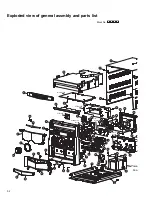
Page 50: ...hone board Front board Vol board VFD board Main board Powe boa AMP board 64 64 24 15 50 26 27 14 66 65 4 20 9 41 30 54 18 20 29 59 62 23 5 8 22 54 61 13 22 11 10 37 12 60 54 49 21 39 55 25 34 52 56 51 36 55 58 7 6 17 33 51 3 57 51 51 32 54 64 35 64 54 2 16 1 64 38 31 5 54 53 ...

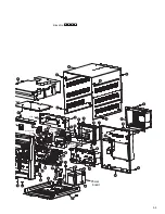
Page 51: ... Front board ard VFD board board Power board AMP board 64 64 24 15 50 26 27 14 40 63 66 65 4 20 9 41 30 54 18 20 29 59 62 23 5 8 22 54 52 56 51 36 55 58 7 6 17 33 51 3 57 51 51 32 54 64 35 64 54 1 64 38 54 64 63 19 52 54 28 31 64 52 54 53 ...

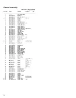
Page 52: ...250V F952 27 BI403011 FUSE 3 15A 250V F951 28 BI202556010101 HEAT SINK 2 29 BI104143010102 HLDR LOCK L 30 BI104143010202 HLDR LOCK R 31 BI202560010101 HLDR R 32 BI202553010101 HLDR L 33 BI107480010101 HLDR SOUND MODE 34 BI202592010101 HOLDER BRACKET 35 BI202555010101 HEAT SINK AMP 36 BI107485010101 INDICATOR STAND 37 BI109819030201 KNOB VOLUME TAB 38 BI202548010101 S METAL COVER 39 BI301922010101 ...

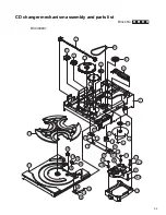
Page 53: ...3 5 CD changer mechanism assembly and parts list 19 21 36 14 7 2 1 3 5 22 37 37 37 37 38B 38A 38B 38A 39 35 32 26 27 29 28 25 34 33 4 6 8 9 10 12 13 11 17 20 15 18 16 24 23 Block No M M M A BI3400931 ...

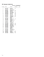
Page 54: ...BI3711003379 CONNECTOR HEADE 16 BIAJ4100601K PCB SW 17 BIAJ6100601K PULLEY MOTOR 1X4 18 BIAJ3100601F MOTOR DC 19 BI3710001248 CONNECTOR SOCE 20 BI3711003692 CONNECTOR HEADE 21 BI3708001163 CONNECTOR FPC 22 BIAJ4100601L PCB MECHA 23 BIAJ7200601P TRAY ROULETTE 1X2 24 BIAJ7200601Q TRAY DISC 1X2 25 BIAJ6600601Q GEAR ROULETTE 1X4 26 BIAJ6600601P GEAR WORM 1X2 27 BIAJ3100601K MOTOR LOADING 28 BIAJ630060...

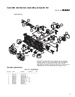
Page 55: ...he whole Cassette Mechanism Assembly Unit When ordering use the Parts No CMAT6Z219A for Cassette Mechanism Assembly Unit L SIDE TYPE R SIDE TYPE Block No M M M P CMAT6Z219A Symbol No Part No Part Name Description Local 1 BIF513858 PLATE HD BLK 2 BIF525346 MTR MAIN BLK 3 BIF567843 PCB CONTROL BLK 4 BIUE20P12 LEAF SWITCH x3 5 BIF522063 CLUTCH ASY BLK x2 6 BIFF19N31 MAIN BELT 7 BIF51435 ROLLIER PINCH...

Page 56: ... Q906 KTC3199GR TRANSISTOR Q907 KTB1366 TRANSISTOR Q909 KRA107M TRANSISTOR Q911 KTC3199GR TRANSISTOR Q912 DTC114ES TRANSISTOR R390 1SS133 DIODE RY301 BI8RL00071 RELAY Symbol No Part No Part Name Description Local CN305 BI1205441U FF CABLE CN306 BI1205261U FF CABLE CN309 BI1205241U FF CABLE CN601 BI1205291U FF CABLE CN604 BI1205251U FF CABLE CN701 BI1205281U FF CABLE DECK BI11AT065B0U WIRE DECKA BI...

Page 57: ...E D5 1SS133 DIODE D50 1SS133 DIODE D51 1SS133 DIODE D6 1SS133 DIODE D605 1N4001 DIODE D7 SVC203 VARASTOR DIODE D8 SVC203 VARASTOR DIODE Symbol No Part No Part Name Description Local D9 1SS133 DIODE IC1 LA1823 IC IC101 TDA7440D IC IC102 BA15218F IC IC2 LC72136N IC IC401 HA12237 IC IC402 M74HC4094B IC IC601 MN6627482WA IC IC611 AN22000A I C C M IC621 BA5936S IC IC631 NJM7808FA IC JA301 BI2301181 RCA...

Page 58: ...T224275M M CAPACITOR F951A BI201196010101 FUSE HOLDER F951B BI201196010101 FUSE HOLDER F952A BI201196010101 FUSE HOLDER F952B BI201196010101 FUSE HOLDER FW951 BI12P90055U CONNECTOR ASSY PWB BI251223G01V TRANS PWB R951 BIRC3352 RESISTOR TB901 BI201323010101 TERMINAL TB902 BI201323010101 TERMINAL ...

Page 59: ...3 11 MEMO ...
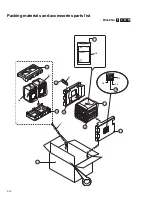
Page 60: ...3 12 Packing materials and accessories parts list FRONT P1 P4 P2 P6 P5 P3 A6 P9 P10 P8 A2 A3 A4 A1 P7 A5 Block No M M M 3 A7 ...

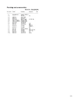
Page 61: ... INSTRUCTIONS LVT1075 001A A 6 MXKA7JW SPBOX L SPEAKER BOX L A 7 MXKA7JW SPBOX R SPEAKER BOX R P 1 BI4313451U CARTON BOX P 2 BI4512251 POLY FORM Left P 3 BI4512261 POLY FORM Right P 4 BI4005355 POLY BAG REMOTE CONTROL P 5 BI4710321 POLY BAG SET P 6 BI4511451 EPE FOAM PAPER SET P 7 BI4710311 POLY BAG INSTRUCTIONS P 8 BI4710511 POLY BAG ANT LOOP P 9 BI4512351 POLY FORM Top P 10 BI4512361 POLY FORM B...

Page 62: ...o improductivity H Others A Completely interchangeable B Previous part can be used for new set but new part can not be used for previous set C New part can be used for previous set but previous part can not be used for new set D Not interchangeable E Addition F Deletion COMMENTS FOB New Parts Itg Rsn Note E H ATTACHMENT NONE COMPONENT PWBLAYOUT SCHEMATIC DIAGRAM ADJUSTMENT PROCEDURE EXPLODED VIEW ...

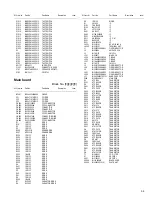
Page 63: ... CAP 150P C418 BICC472500KA034 CHIP CER CAP 4700 P C518 BICC472500KA034 CHIP CER CAP 4700 P C417 BICC471500JA041 CHIP CER CAP 470P C517 BICC471500JA041 CHIP CER CAP 470P C307 BICC821500KA042 CHIP CER CAP 820P R107 BIRC0000165A005 1 16W 0 R207 BIRC0000165A005 1 16W 0 R413 BIRC0000165A005 1 16W 0 Main board Item Parts number Parts name Remarks R513 BIRC0000165A005 1 16W 0 R309 BIRC1000165A005 1 16W ...

Page 64: ...040165A005 1 16W 100K R358 BIRC1040165A005 1 16W 100K R306 BIRC1050165A005 1 16W 1M R109 BIRC1220165A005 1 16W 1 2K R209 BIRC1220165A005 1 16W 1 2K R333 BIRC1510165A005 1 16W 150 OHM R336 BIRC1510165A005 1 16W 150 OHM R364 BIRC1530165A005 1 16W 15K R105 BIRC1540165A005 1 16W 150K Main board Item Parts number Parts name Remarks R205 BIRC1540165A005 1 16W 150K R424 BIRC1820165A005 1 16W 1 8K R349 BI...

Page 65: ... R648 BIRC1030165A005 1 16W 10K R660 BIRC3330165A005 1 16W 33K R621 BIRC1040165A005 1 16W 100K R617 BIRC1050165A005 1 16W 1M R623 BIRC1240165A005 1 16W 120K R605 BIRC2210165A005 1 16W 220 Main board Item Parts number Parts name Remarks R664 BIRC2210165A005 1 16W 220 R663 BIRC2220165A005 1 16W 2 2K R626 BIRC2240165A005 1 16W 220K R620 BIRC2240165A005 1 16W 220K R645 BIRC2240165A005 1 16W 220K R625 ...

Page 66: ...104250ZA043 CHIP CER CAP 0 1UF C717 BICC104250ZA043 CHIP CER CAP 0 1UF Front board Item Parts number Parts name Remarks R775 BIRC1020165A005 1 16W 1K C711 BICC220500JA041 CHIP CER CAP 22P C712 BICC220500JA041 CHIP CER CAP 22P C708 BICC330500JA041 CHIP CER CAP 33P C707 BICC390500JA041 CHIP CER CAP 39P C701 BICC104250ZA040 CHIP CER CAP 0 1UF R778 BIRC1020165A005 1 16W 1K R788 BIRC1020165A005 1 16W 1...

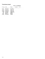
Page 67: ...M R139 BIRC1020085M000 Resistor 1K OHM R239 BIRC1020085M000 Resistor 1K OHM R314 BIRC4740085M000 Resistor 470K OHM R120 BIRC3020045M000 Resistor 3K OHM R220 BIRC3020045M000 Resistor 3K OHM R909 BIRC5630085M000 Resistor 56K OHM R386 BIRC1000085M000 Resistor 10 OHM R387 BIRC1500085M000 Resistor 15 OHM R125 BIRM0022N35P015 Resistor 0 22 3W R126 BIRM0022N35P015 Resistor 0 22 3W R225 BIRM0022N35P015 Re...

Reviews: