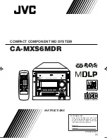
background image

1-1

CA-MXS6MDR

SP-MXS6MD

SERVICE MANUAL

COMPACT COMPONENT MD SYSTEM

No.20876

Sep. 2000

COPYRIGHT      2000 VICTOR COMPANY OF JAPAN, LTD.

CA-MXS6MDR

SP-MXS6MD

CA-MXS6MDR
SP-MXS6MD

Contents

Safety precautions
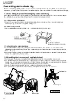
Preventing static electricity
Important for laser products
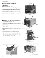
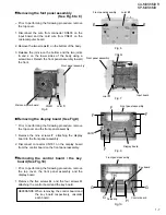
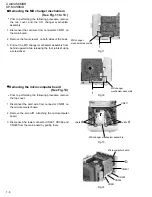
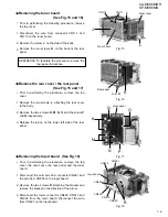
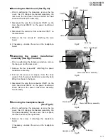
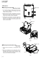
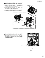
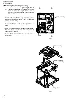
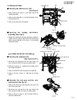
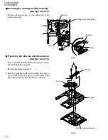
Disassembly method
Adjustment method
Flow of functional operation 
     until TOC read (MD section)

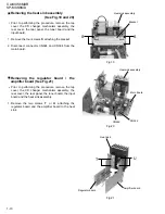
Maintenance of laser pickup (MD)
Replacement of laser pickup (MD)
Flow of functional operation 
     until TOC read (CD section)
Maintenance of laser pickup (CD)
Replacement of laser pickup (CD)
Description of major ICs

1-2
1-4
1-5
1-6
1-31

1-37

1-38
1-38

1-39
1-40
1-40
1-41

Area Suffix

This service manual is printed on 100% recycled paper.

B
E
EN

U.K.

Continental Europe

Northern Europe

COMPACT

DIGITAL AUDIO

DISC LOADING MECHANISM

STANDBY

/ON

LONG
MODE

REC

MODE

SP/LP2/LP4

REC PAUSE

HIGH SPEED

CD  MD

TITLE/EDIT

ENTER

/DEMO

PHONES

LINE 2

MENU

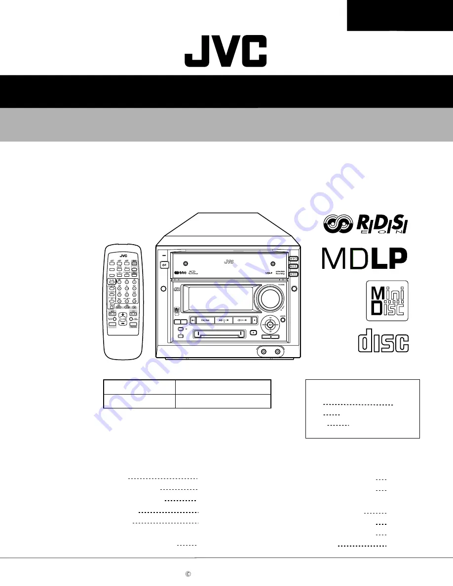
COMPACT COMPONENT MD SYSTEM MX-S6MDR

DISC

DIMMER

LINE

RM-SMXS6MDR

   REMOTE   CONTROL

LEVEL

METER

CA-MXS6MDR

SP-MXS6MD

MAIN SYSTEM

SPEAKER SYSTEM

Summary of Contents for CA-MXS6MDR

Page 1: ...p MD Flow of functional operation until TOC read CD section Maintenance of laser pickup CD Replacement of laser pickup CD Description of major ICs 1 2 1 4 1 5 1 6 1 31 1 37 1 38 1 38 1 39 1 40 1 40 1 41 Area Suffix This service manual is printed on 100 recycled paper B E EN U K Continental Europe Northern Europe COMPACT DIGITAL AUDIO DISC LOADING MECHANISM STANDBY ON LONG MODE REC MODE SP LP2 LP4 ...

Page 2: ...age currnet check Electrical shock hazard testing After re assembling the product always perform an isolation check on the exposed metal parts of the product antenna terminals knobs metal cabinet screw heads headphone jack control shafts etc to be sure the product is safe to operate without danger of electrical shock Do not use a line isolation transformer during this check Plug the AC line cord d...

Page 3: ...perty damage resulting therefrom 3 Essential safety critical components are identified by on the Parts List and by shading on the schematics and must never be replaced by parts other than those listed in the manual Please note however that many electrical and mechanical parts in the product have special safety related characteristics These characteristics are often not evident from visual inspecti...

Page 4: ... the replacement optical pickup are shorted After replacement return the shorted parts to their original condition Refer to the text 2 Do not use a tester to check the condition of the laser diode in the optical pickup The tester s internal power source can easily destroy the laser diode 1 2 Handling the traverse unit optical pickup 1 Do not subject the traverse unit optical pickup to strong shock...

Page 5: ...erstrålning är denna del är öppnad och spårren är urkopplad Betrakta ej strålen VARO Avattaessa ja suojalukitus ohitettaessa olet alttiina näkymättömälle lasersäteilylle Älä katso säteeseen ADVARSEL Usynlig laserstråling ved åbning når sikkerhedsafbrydere er ude af funktion Undgå udsættelse for stråling ADVARSEL Usynlig laserstråling ved åpning når sikkerhetsbryteren er avslott unngå utsettelse fo...

Page 6: ... CN661 on the input board Remove the four screws C on the upper side of the body Remove the screw D on the left side of the body Release the wires from the clamp on the right side of the CD changer mechanism assembly Lift up the rear part of the CD changer mechanism assembly and pull out it from the front assembly 1 2 3 4 Removing the CD changer mechanism assembly See Fig 3 to 5 Fig 1 Fig 2 Fig 3 ...

Page 7: ...lay board to the front panel assembly Disconnect connector CN791 on the display board from the control board on the front panel assembly 1 2 Removing the display board See Fig 9 Prior to performing the following procedure remove the top cover the front panel assembly and the display board Remove the five screws G and the four screws H attaching the control board and the key board 1 Removing the co...

Page 8: ...moving the MD changer mechanism See Fig 11 to 13 Prior to performing the following procedure remove the top cover Disconnect the card wire from connector CN801 on the microcomputer board Remove the screw D attaching the microcomputer board Disconnect the lower connector CN391 CN392 and CN393 from the main board by pulling them 1 2 3 Removing the microcomputer board See Fig 14 MD changer mechanism ...

Page 9: ... 2 3 Remove the rear cover the rear panel See Fig 15 and 17 Prior to performing the procedure remove the top cover the rear cover the rear panel and the tuner board Disconnect the card wire from connector CN661 and the wire from CN603 on the input board Remove the two screws R attaching the bracket and remove the bracket in the direction of the arrow Disconnect the lower connector CN602 CN913 and ...

Page 10: ...ink assembly See Fig 19 and 20 Prior to performing the procedure remove the top cover the CD changer mechanism assembly the rear cover the rear panel the tuner board the input board and the heat sink assembly Remove the two screws T or U attaching the regulator board and the amplifier board to the heat sink 1 Removing the regulator board the amplifier board See Fig 21 Heat sink assembly Heat sink ...

Page 11: ...uner board and the input board Remove the screw X attaching the headphone board If necessary unsolder the wire on the headphone board 1 Removing the headphone board See Fig 25 Prior to performing the following procedure remove the top cover and the rear cover Remove the four screws W attaching the power transformer assembly Pull out the power cord stopper from the body upward Turn the power transf...

Page 12: ...rom connector CN321 and CN451 on the underside of the main board Then remove the main board 1 2 3 Removing the main board See Fig 1 and 2 Remove the four screws B on both sides of the body Move the mechanism cover toward the front to disengage the front hook of the mechanism cover from the internal loading assembly Joint c Then remove the mechanism cover upward 1 2 Removing the mechanism cover See...

Page 13: ... lifter with the spring If necessary remove the spring from the head lifter 1 2 3 Removing the head lifter See Fig 4 to 6 Remove the screw C on the upper side of the body Remove the head assembly while pulling the flexible harness from the body 1 Removing the head assembly See Fig 7 Fig 4 Fig 5 Fig 6 Fig 7 C Head lifter Spring Spring Head lifter Head assembly Head lifter ...

Page 14: ...to disengage it from the traverse mechanism assembly Joint d Then remove it upward Remove the traverse mechanism assembly from the single flame 1 2 3 Removing the Loading assembly See Fig 8 and 9 The loading assembly the traverse mechanism assembly and the single flame will be removable after removing the loading assembly from the body Ref Fig 8 Fig 9 D Loading assembly Joint d D D Loading assembl...

Page 15: ...taching the loading motor and release the joint f Remove the belt from the loading motor assembly Remove the two screws G attaching the loading motor 1 2 3 4 Removing the loading motor See Fig 12 and 13 Loading mechanism assembly Remove the slit washer attaching the cam gear and pull out the cam gear Disconnect the harness from the wire holder and from connector CN612 on the cam switch board Remov...

Page 16: ...cartridge holder assembly Remove the slide bar upward Move the eject bar outward until it stops as shown in Fig 14 Push the convex part g on the bottom of the body and remove the eject bar from the chassis 1 2 Removing the slide bar and the eject bar See Fig 14 and 15 Fig 14 Fig 15 I I I Slide bar Slide bar Eject bar Part g Cartridge holder assembly Cartridge holder assembly Eject bar Eject bar k ...

Page 17: ...Detach the shaft side of the pickup unit upward and release the joint h with the pickup guide Then remove the pickup unit with the shaft 1 2 3 Removing the pickup unit See Fig 17 Draw out the shaft from the pickup Remove the two screws K attaching the rack spring 1 2 Removing the pickup See Fig 18 Traverse mechanism assembly Fig 16 Fig 17 Fig 18 K J Insulators Insulators Joint h Pickup guide Picku...

Page 18: ...he feed motor bracket 1 2 3 Removing the feed motor assembly See Fig 19 1 19 2 Prior to performing procedure remove the feed motor assembly For the red and black harnesses extending from the spindle motor unsolder the soldering j on the traverse mechanism board Remove the screw M attaching the traverse mechanism board 1 2 Removing the traverse mechanism board See Fig 19 1 Fig 19 1 Fig 19 2 M L N F...

Page 19: ...two screws I Fig 20 and 21 1 2 3 Reattaching the loading assembly Make sure the pin of the eject lever marked l is fitted to the slot of the eject bar marked m at the bottom of the loading mechanism chassis after moving the eject lever and the loading slider of the cartridge holder assembly in the direction of the arrow Refer to Fig 21 ATTENTION Fig 20 Fig 21 I I H H UD base UD base Bottom Ditch m...

Page 20: ...t washer while fitting the cam gear slot to the cam switch boss Fig 22 4 5 6 Reattach the loading motor assembly using the screw F Connect the harness extending from the loading motor to connector CN612 on the switch board and fix it with the wire holder Fig 22 7 When reattaching the cam gear the cam switch boss should be fitted to the cam gear slot and the triangle mark of the cam gear should be ...

Page 21: ...de base R while fitting the two pins on another side of the UD base to the slots of the slide base L Fig 25 Make sure the two slots of the slide base L are fitted to the two bosses marked E and tighten the two screws E Fig 26 10 Fit the part v of the slide base R to the part w on the inward side of the cam gear rib Fig 25 ATTENTION To expedite the work bring up the UD base slightly when fitting ea...

Page 22: ...he underside of the servo control board Disconnect the flexible wire from connector CN601 and remove the servo control board from the body 1 2 3 4 5 6 7 Removing the servo control board See Fig 1 to 4 In case of disconnecting the flexible wire without soldering the CD pick up may be damaged ATTENTION When reassembling make sure the cam switch boss of the servo control board is fitted to the slot p...

Page 23: ...on the right side of the body to eject the tray unit From the top of the body release the tray from the joint hook marked d Push the tray toward the front Release the stoppers on both sides in the direction of the arrow and pull out the tray unit from the body 1 2 3 4 5 Removing the tray unit See Fig 5 to 8 Pull out the tray unit from the top tray 3 in sequence ATTENTION Fig 5 Fig 6 Fig 7 Fig 8 B ...

Page 24: ...assis unit is located at the top position ATTENTION Turn the hook gear counterclockwise to move the slide hook and the slider R backward until they stop Remove the three screws D attaching the side unit R Raise the side unit R upward and release the joint g with the chassis unit and the boss from the select arm marked h Then remove the side unit R from the body 4 5 When reassembling make sure the ...

Page 25: ... the arrow until they stop The notches of each slide cam are fitted to the pins on both sides of the sub chassis unit Detach the sub chassis unit upward 1 2 3 Removing the sub chassis unit See Fig 10 to 12 When reassembling turn the hook gear of the chassis unit counterclockwise until it stops and slide the slide hook and the slider R of the sub chassis unit backward until they stop ATTENTION Fig ...

Page 26: ...belts from the two pulleys on the gear base unit Remove the three screws F and remove the gear base unit from the body 1 2 3 Removing the flap base unit and the gear base unit See Fig 13 and 14 Prior to performing the following procedure remove the main board Remove the belts from the two pulleys Remove the four screws G and detach each motor from the body 1 2 Removing the motors See Fig 15 Fig 13...

Page 27: ...t m with the pickup holder Detach the pickup with the screw shaft Solder the part n of the flexible board on the underside of the pickup After soldering disconnect the flexible wire connected to the pickup In case of disconnecting the flexible wire without soldering it may cause damage to the CD pickup Remove the two screws J attaching the rack arm to the pickup unit Pull out the screw shaft from ...

Page 28: ...llowing procedure remove the traverse mechanism assembly Remove the screw L attaching the feed motor 1 Removing the feed motor See Fig 22 Fig 21 Fig 22 K K K Traverse mechanism assembly Traverse mechanism assembly Joint o Feed motor L Fig 23 Tray select switch board CN620 M Fig 5 Fig 6 B Top cover B Rod Clamper base unit Top cover Rod Clamper base unit Remove the four screws B attaching the top co...

Page 29: ...ment grille is damaged replace it with the woofer ATTENTION Prior to performing the following procedure remove the front grille When replacing the ornament grille make sure the boss with adequate amount of bond ATTENTION Speaker section Information This is a method of dis assembly As parts of the repair of this speaker system it is only the speaker box assemblies It is not possible to supply with ...

Page 30: ...e body 1 Remove the three screws B and the tweeter from the body Disconnect the wire from the speaker terminals 3 Removing the speaker tweeter See Fig 4 and 5 As the ornament grille is damaged replace it with the tweeter ATTENTION Fig 4 Fig 5 Driver Ornament grille Tweeter Tweeter B B A A Woofer ...

Page 31: ...DING laser power 0 68mW Adjustment 2 Initialize the EEPROM Setting the MD TEST MODE 1 Press REC PAUSE key of the Remote controller LCD indication DATA INITIAL Initialize OK Laser power up by key of Remote controller Laser power down by key of Remote controller Laser power up by key of Remote controller Laser power down by key of Remote controller Press 4 key of Remote controller LCD indication L P...

Page 32: ...ey of the main body NG code list CODE 00 01 02 03 04 05 06 07 08 09 0A 0B 0C 0D 0E FF Adjustment NG section Auto adjustment not complete REST switch detection FOCUS ON PIT section EF balance tracking offset adjustment PIT section ABCD level IV impedance adjustment PIT section focus servo AGC PIT section tracking servo AGC PIT section focus bias adjustment GRV section EF balance tracking offset adj...

Page 33: ...on the drift level of the pickup adjustment value 4 Release the MD TEST MODE TEST MODE 2 Read the TOC Press 8 key of the Remote controller LCD indication change by each 10sec _ _ _ _ _ Insert the recordable disc basically 74min LCD indication change be each 10sec ______ Times_ 3 Indication the C1 ERROR Adjustment value IVR TAGC TBAL LPOW FBIA FAGC TEOF SAGC IVR Pre master Recordable groove TRK AGC...

Page 34: ...ether and connect the power cord Release the TEST MODE 3 Release the CD TEST MODE TEST MODE Read TOC Press 1 key of the Remote controller x1 speed Press 2 key of the Remote controller x2 speed Playback each 10sec C1 ERROR q ty indicate by 2byte 2 Indication the C1 ERROR LCD indication change each 10sec __________ __ LCD indication change each 10sec ________ Times__ TEST MODE Press POWER key Power ...

Page 35: ...full color LED RED 1 Setting the TEST MODE 2 Fast forward of CLOCK SLEEP TIMER press any key Change to normal indication It can check for red color chip part Inspection for static electricity broken check mode for full color LED GREEN It can check for green color chip part Inspection for static electricity broken check mode for full color LED BLUE It can check for blue color chip part Caution Full...

Page 36: ...t IC801 6 7 9pin when system CPU IC801 supply voltage US D5 6V is normal condition Watching the abnormal at POWER ON condition if detect the abnormal indicate CAUTION and come under stability power supply 8V 10V or 12V OR 6V and indicate DATA HEX of the abnormal port voltage then power off to forcibly Detect the abnormal condition of stability power supply is next 8V 10V SAFETY1 port Power supply ...

Page 37: ...rotated Confirm that the Focus error S curve signal at the pin 34 of IC310 is approx 2Vp p TOC reading Play a disc Automatic tuning of Tracking error gain Automatic tuning of Focus error gain Confirm that the eye pattern at the pin38 of IC310 Check point Confirm that the voltage at the pin 50 of IC500 are 4V Confirm that the voltage at the pin 9 of CN408 are 0V It is confirmed that pin 2 of CN408 ...

Page 38: ...p to TEST mode according to the procedures described in the adjustment method Adjust the laser power Completion the disc Completion of changing the MD pickup Since this system is designed to perform magnetic recording the laser power ten times or over of the conventional MD player will be output Therefore be sure to perform not only adjustment and operation of this system so carefully as not to di...

Page 39: ...rox 3sec IC601 25pin TE Approx 1 8V VREF Tracking error waveform at TOC reading Power ON Disc play Key Confirm that the Focus error S curve signal at the pin28 of IC603 is approx 2Vp p Confirm that the signal form pin24 of IC603 is 0V as a accelerated pulse during approx 400ms Confirm the waveform of the tracking error signal at the pin25 of IC601 about 1 8Vpp FO gain auto adjust TE gain auto adju...

Page 40: ...is time check that the laser emits for about 3seconds and the objective lens moves up and down CAUTION Do not observe the laser beam directly Play disc Check the eye pattern at TP602 Finish Maintenance of laser pickup CD Is RF output 1 25 0 22VP P 3 Semi fixed resistor on the APC board The semi fixed resistor on the APC board which is attached to the pickup is used to adjust the laser power Since ...

Page 41: ...CLK SDTO DGND VD SDTI CMODE DEM1 DEM0 AOUTL AOUTR VCOM AGND VB VA Voltage Reference Input Pin for DAC VA Voltage Reference Input Pin for ADC VA RCH Analog Input Pin Rch Common Voltage Output Pin 0 45xVA Lch Common Voltage Output Pin 0 45xVA Lch Analog Input Pin ADC Power Down Mode Pin L Power Down DAC Power Down Mode Pin L Power Down Master Clock Input Pin Input Output Channel Clock Pin Audio Seri...

Page 42: ...2 CA MXS6MDR SP MXS6MD DET BDO OFTR GCTRL DET AGC EQ 17 10 9 8 6 5 3 36 35 34 33 32 31 30 28 11 12 Substraction Substraction FBAL TBAL 29 16 15 14 13 AN8849SB W IC601 Head amp 1 Pin layout 2 Block diagram ...

Page 43: ...gnal output terminal RF signal amp detection output Ground LD APC ON OFF select Reference voltage output terminal CROSS detect signal output terminal Reference voltage output terminal CROSS detect filter connect terminal Tracking error output terminal TE amp negative input terminal FE amp negative input terminal Focus error output terminal Focus gain tracking gain adjust control signal inout termi...

Page 44: ...utput A current input for main beam servo signal B current input for main beam servo signal C current input for main beam servo signal D current input for main beam servo signal E current input for side beam servo signal F current input for side beam servo signal Reflection light quantity monitor signal input Laser APC output Reference voltage input for the laser power intensity setting Connect to...

Page 45: ...nal output Reflection light quantity signal output for the main beam servo detector RF ABCD bottom hold signal output Peak hold signal output for the RF ABCD signals RF equalizer output Connects the RFAGC capacitor RFAGC input User comparator output User comparator non inverted input Connects the capacitor for ADIP amplifier feedback circuit User operational amplifier output User operational ampli...

Page 46: ... GENERATOR 16 17 18 29 27 28 90 52 OSCI OSCO XTSL FS256 LRCK XBCK FS4 MDDT1 SHOCK RESISTANT MEMORY CONTROLLER ATRAC ATRAC3 ENCODER DECODER DIGITAL AUDIO I F SAMPLING RATE CONVERTER SUBCODE PROCESSOR 4 4 4 12 2 46 44 47 43 XRAS XCAS XWE XOE A00 A11 D0 D3 14 15 XINT TX 26 25 24 23 22 21 DADT ADDT XBCKI LRCKI DATAI DIN DIN1 DOUT 12 11 DQSY SQSY 84 88 89 86 85 92 91 83 LDDR FFDR FRDR TFDR TRDR SFDR SR...

Page 47: ...XTSL high 512Fs 22 5792MHz XTSL1 command low and XTSL low 1024Fs 45 1584MHz XTSL1 command high 2048Fs 90 3168MHz Digital audio interface signal input 1 Digital audio interface signal input 2 Digital audio interface signal output Test pin Connect to GND Test pin Connect to GND Test pin Connect to GND Data input from A D converter REC monitor output decoded audio data output LA clock 44 1kHz output ...

Page 48: ... quantity of light Signal input for quantity of light Focus error signal input Auxillary input 1 Center voltage input Monitor output for A D converter input signal Analog power supply Voltage input for the upper limit of the A D converter operating range Voltage input for the lower limit of the A D converter operating range Analog ground Sled error signal input Tracking error signal input Connect ...

Page 49: ...k EFM encoded data output when recording SRDR SFDR SPRD SPFD FGIN TEST1 TEST2 TEST3 DVSS EFMO O O O O I I I I O Pin No Symbol I O Function 1 2 3 4 5 6 7 14 13 12 11 10 9 8 IN OUT1 OUT IN1 OUT IN2 IN OUT2 CONT2 CONT3 VSS VDD CONT1 CONT4 IN OUT4 OUT IN4 OUT IN3 IN OUT3 O I I O CONT TC4066BP N IC673 Switch 1 Pin layout block diagram 2 The truth circuit 1 2 3 4 5 6 7 14 13 12 11 10 9 8 1Y 1A 1B 2Y 2A ...

Page 50: ...CDX2662R Non connected Power supply Ground AD power control output DA power control output Emphasis control output Non connected High frequency ON OFF output High frequency power select output Non connected Data output for debag test mode Clock output for debag test mode Latch output for debag test mode Input frequency select output to CXD2662R Ground Write data output permission to CXD2662R Non c...

Page 51: ... CPU Test terminal Operation setting for CPU Operation setting for CPU Reset input of CPU Oparation setting for CPU Oparation setting for CPU Power supply terminal X tal OSC terminal 10MHz X tal OSC terminal 10MHz Ground Non connect Magnetic head driver ON OFF CD emphasis input CD Cbit input CD TNO input Sub code Q A dip syne Connect to CXD2662R DQSY Interrupter requier Power supply Power supply M...

Page 52: ...LD MCLK MDATA DSL PLL VCO AVDD2 SUB CODE BUFFER SSEL SQCK SUBQ AVDD2 CLVS CRC BLKCK CLDCK SBCK SUBC DEMPH RESY FLAG6 RESY EFM DEMODULATION SUBCODE DEMODULATION SYNC INTERPOLATION 16k SRAM CIRC ERROR CORRECTION DEINTERLEVE LRCKIN MSEL BCLK SSEL SRDATAIN PSEL IOSEL DIGITAL DEEMPHSIS 8TIMES OVER SAMPUNC DIGITAL FILTER 1BIT DAC LOGIC S PEM R PEM L DIGITAL AUDIO INTERFASE DIGITAL AUDIO INTERFASE INTER ...

Page 53: ...ror signal output Kick pulse output Tracking drive output Focus drive output Reference voltage input pin for D A output block TVD FOD FBA TBAL Focus Balance adjust signal output Tracking Balance adjust signal output Focus error signal input Analog input Tracking error signal input Analog input RF envelope signal input Analog input Vibration detect signal input H detect Off track signal input H off...

Page 54: ...power supply voltage Rest switch CD emphasis CD track No change CD copy right or wrong Sub Q data input Cam position 1 Sub Q clock output Command signal input Status output Command data clock input Command in Status out Cam position 2 Reference power supply 1 Ground key1 signal from running jig Key2 signal from running jig Tray 3 close signal input Tray 3 open signal input Tray 2 close signal inpu...

Page 55: ...se Actuator motor rotation counter clockwise Actuator motor rotation clockwise Gain select 2 4 speed Equalizer select 2 4 speed Cam position 3 Cam position 4 Reset signal output Status signal input Digital mute signal input Power on signal input Command load signal input Command data input Command clock input Communication select signal input Running data input from running jig Running load 2 sign...

Page 56: ...O DI CS SK PE 1 2 3 4 PE VCC CS SK NC GND DO DI 8 7 6 5 8 PIN SOP Pin no Symbol 1 PE 2 VCC 3 CS 4 SK 5 DI 6 DO 7 GND 8 NC Function Program enable With built in pull up resistor Power supply Chip selection Cereal clock input Cereal data input Cereal data output Ground No connection NOTE The pull up resistor of the PE pin is about 2 5M VCC 5V AK93C65AF X IC590 EEPROM 1 Pin layout 2 Block diagram 3 P...

Page 57: ... Reg NF Non connect Sync output Lower power MOS drain H bridge GND Lower power MOS source Sync output Lower power MOS drain Source output Upper power MOS source H bridge power supply terminal Upper power MOS source Source output Upper power MOS source External PNP drive output for regulator Reglator output Emitter follower output Regulator feedbaack terminal I I O I I O O O O O O O O Pin No Pin No...

Page 58: ...N Vcc LEVEL DETECT ACK START STOP BR24C01AFV W X IC201 EEPROM 1 Pin layout 2 Block diagram 3 Pin function A0 A1 A2 GND Vcc WP SCL SDA Pin name I O Function Vcc GND A0 A1 A2 SCL SDA WP IN IN IN OUT IN 1 An open drain output requires a pull up resister Power supply Ground 0v Slave address set Serial clock input Slave and word address serial data input serial data output 1 Write protect input ...

Page 59: ...Enable Address Input 4K Refresh Product Address Input 2K Refresh Product Data In Out Power 3 3V Ground No Connection Vcc Vss Substrate Bias Generator X16 Parallel Test RAS Clock Generator Row Presecoder 11 12 11 12 RAS Refresh Counter Refresh Counter Address Buffer Cloumn Predecoder 11 12 CAS Clock Generator Data Input Buffer DQ0 3 DQ0 3 4 4 4 4 Data Output Buffer 11 10 Row Decoder Memory Array 4 ...

Page 60: ...r outputs ON OFF BTL AMP 1 input pin BTL AMP 1 input pin For gain adjustment BTL AMP 1 input pin Non inverting side BTL AMP 1 input pin Inverting side BTL AMP 2 input pin Inverting side BTL AMP 2 input pin Non inverting side BTL AMP 2 input pin For gain adjustment BTL AMP 2 input pin External transistor collector PNP connection 5V power supply output External transistor PNP base connection Reset o...

Page 61: ...3 14 12 8 9 7 6 5 3 4 39 38 40 37 41 42 34 35 31 30 23 24 22 29 28 26 25 27 19 17 18 10 11 32 33 IN1 IN1 OUT1 VM1 VM1 VM2 VM2 OUT2 IN2 I IN2 VREFO VREF REGB REG VREF E2 CH2 X5 CH1 X5 E1 VREG VBS1 VBS1 VBS1 VBS2 VBS1 VBS1 VBS2 1 25V CH3 X8 CH4 X8 CH5 X8 E3 E4 E5 VBS2 VBS2 VBS2 VBS2 Vm1 Vm2 R R R R Vrefm1 Vrefm2 BIAS HI Sleep SLEEP TSD Low Open MUTE ON 1 4 CH 5CH VBS1 Vm1 VBS1 VBS2 Vm2 IN3 IN3 OUT3 ...

Page 62: ...Connect to ground Connect to ground MD RED output terminal Connect to ground Commor signal output terminal Commor signal input terminal Commor clock signal input terminal Connect to ground Write enable output terminal Read enable output terminal Chip select output terminal Connect to ground Connect to ground Data select signal output terminal LCD reset signal output terminal Connect to ground Dimm...

Page 63: ...1 63 CA MXS6MDR SP MXS6MD V INPUT V OUTPUT A OUT A IN A IN V 1 2 3 4 A B TOP VIEW 8 7 6 5 V B IN B IN B OUT 1 Terminal layout 2 Block diagram NJM4580D IC672 LPF Mic and H phone Amp ...

Page 64: ... 1 4 R1 TR1 TR3 TR2 TR4 TR5 TR6 TR8 R8 C2 TR14 TR15 TR16 R14 R11 R13 R12 R10 R9 TR9 TR10 TR12 TR13 TR11 TR7 C1 D1 R6 R3 R4 R5 R7 13 11 14 15 9 8 12 5 6 7 10 2 R2 SUB STK402 030 IC301 Power amp 1 Pin layout 2 Block diagram 1 15 ...

Page 65: ...Y A A TC7S32F X IC603 NAND gata 1 Pin layout 2 Block diagram 1 2 3 4 5 6 7 8 9 10 GND OUT1 P1 VZ IN1 IN2 VCC1 VCC2 P2 OUT2 Input Output Mode IN1 IN2 OUT1 OUT2 Brake 0 0 0 0 1 0 1 0 0 1 0 1 1 1 0 0 CLOCKWISE COUNTER CLOCKWISE Brake LB1641 IC851 IC852 DC motor driver 1 Pin layout 2 Pin function A OUT 1 A IN 2 A IN 3 V 4 8 V 7 B OUT 6 B IN 5 B IN NJM4580E W IC652 Ope amp ...

Page 66: ...VOLUME VOLUME TREBLE TREBLE MIDLE MIDLE SPEAKER ATT RIGHT SPEAKER ATT LEFT BASS BASS SUPPLY G G I C BUS DECODER LATCHES 2 0 30dB 2dB STEP INPUT MULTIPLEXER GAIN CSL DIG GND TREBLE R TREBLE L MIN L MOUT L BOUT L BIN L BOUT R BIN R MOUT R MIN R INR MUXOUTR INL SDA CRE Vs AGND ROUT LOUT R IN4 R IN3 R IN2 R IN1 L IN1 L IN2 L IN3 L IN4 MUXOUTL TDA7439 1 2 3 4 5 6 7 8 9 10 11 12 13 14 15 30 29 28 27 26 ...

Page 67: ...al Sensor Cnp Bandgap Reference GND VIN Rin 550k on off Ccont TK11140SC W IC485 Regulator 1 Pin layout 2 Block diagram OUT1 1 Ii1 2 IN1 3 V 4 8 V 7 OUT2 6 Ii2 5 IN2 1 2 IN Ii Q1 Q2 Q5 Q6 Q3 Q4 Q7 Q8 V OUT V 100 A 100 A UPC393G2 W IC602 Voltage comparator 1 Pin layout 2 Block diagram ...

Page 68: ...rent Limit Voltage Reference XC62ER3602M X IC400 Regulator 1 Pin layout 2 Block diagram 3 Pin function 1 5 4 2 3 1 2 3 4 5 GND Power supply input Regulator output Base current control terminal Chip enable V V V EXT CE Pin No Symbol Function SS IN OUT ...

Page 69: ...P MXS6MD Printed in Japan 200009 O No 20876 CA MXS6MDR SP MXS6MD VICTOR COMPANY OF JAPAN LIMITED AUDIO COMMUNICATION BUSINESS DIVISION PERSONAL MOBILE NETWORK B U 10 1 1Chome Ohwatari machi Maebashi city 371 8543 Japan ...

Reviews: