background image

(No.YF335<Rev.001>)1-15

z

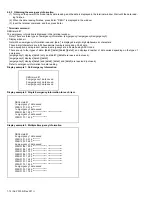
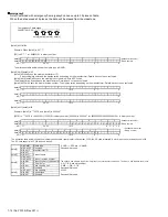
emergency3

Note) Combined with emergency2, emergency3 can save up to 32 pieces of data.
When the data exceeds 32 pieces, the data will be erased from the oldest one. 

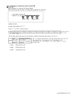
data[0]

31

28 27

25 24 23

12 11

0

SDVideo

Error type

0: HDD error / 1: Unsupported file / 3: Failed playback file / 4: Unknown error

Media type

0: HDD or NAND / 1: SD card

SDVideo / User MPEG 0: SD Video / 1: User MPEG
Folder number

1-0xFFF

File number

1-0xFFF

User MPEG

Note) User MPEG is the data handled as another file due to no management file.

Error type

0: HDD error / 1: Unsupported file / 3: Failed playback file / 4: Unknown error

Media type

0: HDD or NAND / 1: SD card

SDVideo / User MPEG 0: SD Video / 1: User MPEG
File number

1-9999

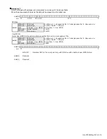
data[1]

31

0

bit0-bit31

Indicates GOP on the error point only with SDVideo with undefined user MPEG value.

data[2]

Reserved

data[3]

Reserved

bit

ψ

bit25-bit27

bit28-bit31

bit0-bit11

bit12-bit23

bit24

bit

ψ

bit0-bit23

bit24

bit25-bit27

bit28-bit31

[data0]

[data0]

Summary of Contents for EVERIO GZ-MS110BEK

Page 1: ... Cu melting point 219 Centigrade This service manual No YF335 Rev 001 describes only the items which differ from those of already issued service manual No YF334 Rev 001 For details other than those described in this manual please refer to the service manuals which were already issued TABLE OF CONTENTS 1 PRECAUTIONS 1 3 2 SPECIFIC SERVICE INSTRUCTIONS 1 5 3 DISASSEMBLY 1 16 4 ADJUSTMENT 1 28 5 TROU...

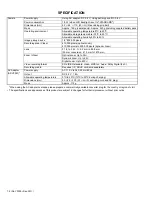
Page 2: ...ble operating temperature 0 C to 40 C Allowable storage temperature 20 C to 50 C Allowable operating humidity 35 to 80 Image pickup device 1 6 800 000 pixels Recording area Video 410 000 pixels optical zoom 410 000 pixels to 550 000 pixels dynamic zoom Lens F 1 8 to F 4 3 f 2 2 mm to 85 8 mm 35 mm conversion 41 5 mm to 1619 mm Zoom Video Optical zoom Up to 39 Dynamic zoom Up to 45 Digital zoom Up ...

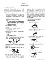
Page 3: ...ed parts 9 When a power cord has been replaced check that 10 15 kg of force in any direction will not loosen it Fig 1 1 2 10 Also check areas surrounding repaired locations 11 Products using cathode ray tubes CRTs In regard to such products the cathode ray tubes themselves the high voltage circuits and related circuits are specified for compliance with recognized codes pertaining to X ray emission...

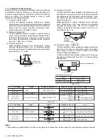
Page 4: ... plug prongs and externally exposed accessible parts Use an AC voltmeter to measure across both terminals of load Z See Fig 1 1 9 and following Fig 1 1 12 Fig 1 1 9 5 Grounding Class 1 model only Confirm specified or lower grounding impedance between earth pin in AC inlet and externally exposed accessible parts Video in Video out Audio in Audio out or Fixing screw etc Measuring Method Connect mill...

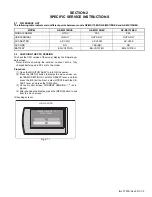
Page 5: ... to turn ON the power 2 Press the MENU button to display the menu screen se lect BASIC SETTINGS with the SELECT lever and then press the OK button Next select UPDATE with the SE LECT lever and press the OK button 3 On the monitor screen CURRENT VERSION is dis played 4 After checking the display press the MENU button to exit from the menu screen Checking screen Fig 2 1 1 MODEL GZ MS110BUS GZ MS110B...

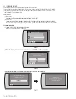
Page 6: ...ation Download the firmware update application software from JS NET 2 Connection Connect a battery that is capable of operating for 30 minutes or longer and an AC adapter to Everio To ensure secure power supply during the update update is disabled if either of them is not available 2 Firmware transfer 1 Select UPDATE in the main menu of Everio MENU BASIC SETTINGS UPDATE Fig 2 2 1 2 When the displa...

Page 7: ... No YF335 Rev 001 1 7 4 Double click the downloaded file to execute it The following shows the screen display of the PC Fig 2 2 4 㬍 㬍 㬍 㬍 㬍 Execute the file Click OK to finesh the file Click YES ...

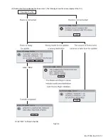
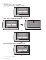
Page 8: ...press OK Fig 2 2 5 3 When the displayed current version is an old one select YES and then press OK It takes about 4 minutes and 30 seconds to complete the update Fig 2 2 6 4 Select OK and then re start Everio Fig 2 2 7 5 After the re start check that the current firmware is updated in UPDATE MENU BASIC SETTINGS UPDATE Fig 2 2 8 When the updated firmware version is confirmed select NO and then pres...

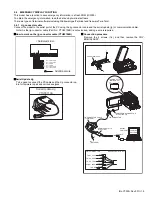
Page 9: ...quired How to work on the jig connector cable YTU93106B Serial Update Jig To be used to connect the PC cable and the Jig connector ca ble for firmware repair and various analyses Connection procedure Remove the 4 screws 1 4 and then remove the COV ER HIN ASSY 11 Additional wire Soldered side 8 RKP NOT USE 9 RKP GND 5 RKP NOT USE 12 RKP NOT USE 11 RKP UA_TXD0 10 RKP GND Serial Update Jig YTU93113A ...

Page 10: ... NC NC NC NC 10 9 8 7 6 5 4 3 2 1 30 29 28 27 26 25 24 23 22 21 20 19 18 17 16 15 14 13 12 11 10 9 8 7 6 5 4 3 2 1 MAIN CN110 JIG CONN BOARD PIN NO ADDITIONAL WIRE JIG CONNECTOR CABLE YTU93106B 15 14 13 12 11 10 9 8 7 6 5 4 3 2 1 KENTO AL_2 83V IF_RX DSP_TCK UA_RXD0 DSP_TDI SYS_RSTL REG_2 83V DSP_RST DSP_RTCK NC NC NC NC NC 1 2 3 4 5 6 7 8 9 10 30 29 28 27 26 25 24 23 22 21 20 19 18 17 16 11 12 13...

Page 11: ...oftware Before starting the terminal software install the terminal software 1 Start Tera Term select Serial and then click OK 2 Select Setup Serial port Set each item and then click OK Maximizing terminal window size enables better viewing of output data ...

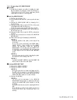
Page 12: ... types of data data0 data1 data2 data3 and displayed number of data varies depending on the type of emergency emgergency1 displays data0 only and data1 data3 are reserved not used emgergency2 displays data0 data3 emgergency3 displays data0 and data2 data2 and data3 are reserved not used Refer to emergency information for data reading Display example 1 No Emergency Information Display example 2 Sin...

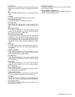
Page 13: ...data 0 Hexadecimal number Binary number data 0 31 30 28 27 0 The allocation table below shows the drop detection setting is ON and the drop distance is 21 40 cm bit31 Drop detection setting 0 OFF 1 ON Indicates the status set on the menu setting screen on the main unit bit28 bit30 Drop distance 0 Drop distance 0 20 1 Drop distance 21 40 2 Drop distance 41 60 Unit cm 3 Drop distance 61 80 4 Drop di...

Page 14: ...ata3 is 002004 09C2 in 09C2 is 0000100111000010 in binary number 002004 in 002004 is 000000000010000000000100 in binary number data 2 data 2 data 3 data 3 31 16 15 8 7 0 The allocation table below shows the media production date year month is December 2009 the SD card is inserted in slot A and the card capacity unit is GB The SD card capacity is 32 GB in speed class 4 0 HDD 1 SDCard 2 NAND Reserve...

Page 15: ...o 1 User MPEG Folder number 1 0xFFF File number 1 0xFFF User MPEG Note User MPEG is the data handled as another file due to no management file Error type 0 HDD error 1 Unsupported file 3 Failed playback file 4 Unknown error Media type 0 HDD or NAND 1 SD card SDVideo User MPEG 0 SD Video 1 User MPEG File number 1 9999 data 1 31 0 bit0 bit31 Indicates GOP on the error point only with SDVideo with un...

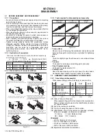
Page 16: ...n 4 Identification of part to be removed unhooked unlocked released unplugged unclamped or unsoldered S Screw L Lock Release Hook SD Solder CN Connector Example 4 S1a Remove 4 S1a screws 3 L1a Disengage 3 L1a hooks 2 SD1a Unsolder 2 SD1a points CN1a Remove a CN1a connector 5 Adjustment information for installation CN2a CN2b MAIN CN101 MAIN CN103 40 10 CONN No PIN No CONNECTOR Two kinds of double a...

Page 17: ... OP BLOCK ASSY from the HOOK L8b and then slide and pull out the STUD L8c 4 Pull out each FPC from the connectors CN8a b in turn NOTE8b To attach the OP BLOCK ASSY insert the FPCs OP BLOCK ASSY into the gap between the HOLDER OP be fore connecting the FPCs to the connector NOTE8c Refer to Fig 3 2 15 and the procedures that follow for disas sembly of OP BLOCK ASSY NOTE11a During the procedure be ca...

Page 18: ... and then tighten the screw 39 NOTE17c Refer to 3 2 3 DISASSEMBLY OF Disassembly of 17 MONITOR ASSY NOTE18a During the procedure be careful in handling the parts NOTE18b During the procedure hold the outer rim of the SPEAKER NOTE18c When attaching the SPEAKER be careful so that the SPEAKER terminal and the BKT SPK do not contact NOTE18d When attaching the SPEAKER be careful in handling the WIRE SP...

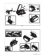
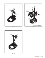
Page 19: ... S1 2 S1 2 S1 L1a JACK COVER SD L1d L1b L1d L1c L1f L1e 3 S1 3 S1 4 S1 4 S1 1 NOTE1c NOTE1a NOTE1b OK Firmly attached hook Misaligned hook NG HOOK 9 S2 10 S2 11 S2 2 5 S2 6 S2 L2a L2f L2d L2c L2b L2e 5 S2 7 S2 8 S2 6 S2 7 S2 8 S2 NOTE2b NOTE2a NOTE2a ...

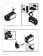
Page 20: ...o YF335 Rev 001 Fig 3 2 3 Fig 3 2 4 Fig 3 2 5 12 S3 3 L4d L4c CN4 CN4 13 S4 SW ZOOM SW TRIG 4 L4a L4b NOTE4 14 S5a 15 S5a 16 S5b L5b CN5 L5a FPC HINGE FPC MIC FPC MIC 5 L5a NOTE5a NOTE5a NOTE5c NOTE5b NOTE5a ...

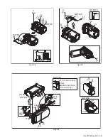
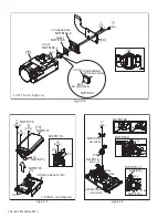
Page 21: ...9 S6b CN6 L6 20 S6b 17 S6a 18 S6a 6 6 NOTE6 NOTE6 21 S7 23 S7 22 S7 21 S7 L7c L7b L7a NOTE7b NOTE7a NOTE7b 7 8 CN8a L8a a b CN8b FPC FPC OP BLOCK ASSY CN8b OP BLOCK ASSY MAIN BOARD ASSY FPC 24 S8 24 S8 25 S8 25 S8 STUD L8c HOOK L8b a b NOTE8a NOTE8b NOTE8c ...

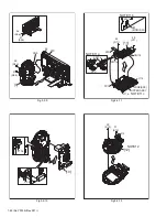
Page 22: ... Fig 3 2 10 Fig 3 2 11 Fig 3 2 12 9 CN9 L9 26 S9a 26 S9a 27 S9b 27 S9b FPC 10 L10b L10a 11 L11a FPC CN11a CN11a CN11b S101 SW MONI SW 28 S11 29 S11 L11b WIRE SPK UPPER ASSY FPC FPC NOTE11b NOTE11a NOTE11c 12 31 S12 L12 30 S12 NOTE12 ...

Page 23: ... No YF335 Rev 001 1 23 Fig 3 2 13 Fig 3 2 14 Fig 3 2 15 13 32 S13 L13b L13a FPC 14 FPC 0 118 N m 1 2kgf cm 15 34 S15 33 S15 FPC FPC HOLDER OPSD ASSY 35 S15 ...

Page 24: ...ENS SIDE OP LPF NOTE16b c NOTE16b NOTE16a b 0 147 N m 1 5kgf cm NOTE16c 17 39 S17b 40 S17b 38 S17a L17b FPC FPC L17a L17a L17c UPPER CASE ASSY SD 38 S17a NOTE17b NOTE17b NOTE17a NOTE17a NOTE17c 0 196 N m 2 0kgf cm 18 41 S18 L18c L18a L18b OK NG BKT SPK UPPER CASE ASSY SD WIRE SPK L18a L18b NOTE18c NOTE18d NOTE18b NOTE18c d NOTE18c NOTE18 a b c d ...

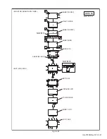
Page 25: ...CD CASE On one side of the LCD CASE the SHEET BEF SHEET M DIFF LIGHT GUIDE and the SHEET M REF are assembled toward the MONITOR BOARD ASSY On the other side the SHEET LCD LCD MODULE and the SPACER LCD are assembled in order between the LCD CASE and the BRACKET LCD NOTE17b During the procedure be careful in handling the parts Be very careful not to damage the FPC NOTE17c To attach the SHEET M DIFF ...

Page 26: ...UNIT HINGE UNIT FPC FPC FPC 5 S17a 6 S17a 3 S17b 1 S17a 2 S17a 4 S17b 3 S17b 4 S17b L17c L17d L17e L17j L17h L17k L17f L17g L17h L17j L17p L17n L17m L17p L17n OK NG L17m L17r L17r L17q N S L17q MONITOR CASE ASSY MONI SA c d e f g h j b a MONITOR COVER ASSY CN17b CN17a NOTE17d NOTE17a b c NOTE17d NOTE17d NOTE17d NOTE17e HINGE UNIT ...

Page 27: ...SHEET M REF LIGHT GUIDE MONITOR BOARD ASSY SIDE MONI SA BKT LCD SIDE e f g h j a b c d a b c d BKT LCD LCD MODULE SHEET M DIFF SHEET BEF SHEET B LIGHT SHEET LCD SPACER LCD LCD CASE v w x u t s r q k m n p v w x u t s r q k m n p v w x u t s r q k m n p BKT LCD e f g h j ...

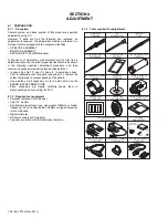
Page 28: ...e pattern Use a patch cord if necessary As for a patch cord see the BOARD INTERCONNECTIONS Since connectors are fragile carefully handle them in disconnecting and connecting the FPC 4 1 2 Required test equipment Personal computer for Windows Color TV monitor Oscilloscope dual trace type observable 100MHz or higher frequency The one observable 300 MHz or higher frequency is recommended Digital volt...

Page 29: ...t lens holder For the usage of the Mini stand refer to the Service Bulletin No YA SB 10035 Light Box Assembly To be used for adjustment of the camera system For the usage of the Light box assembly refer to the Service Bulletin No YA SB 10035 and No YA SB 10218 Color Bar Chart To be used for adjustment of the camera system For the usage of the INF adjustment lens refer to the Service Bulletin No YA...

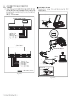
Page 30: ...then remove the COV ER HIN ASSY Fig 4 2 2 ADDITIONAL WIRE 13 22pin NOT USED 23pin NOT USED 26pin NOT USED 28pin IF_RX 29pin AL_2 83V 8pin NOT USED 9pin GND 5pin NOT USED 13pin IF_TX 12pin NOT USED 10pin GND 28 COMPONENT SIDE FOIL SIDE 1 2 4 3 COVER HIN ASSY 10 20 1 11 PC CABLE COMMUNICATION CABLE JIG CONNECTOR CABLE MENU RS232C COM PORT SERVICE SUPPORT SYSTEM PERSONAL COMPUTER COMMUNICATION CABLE ...

Page 31: ...RSTL GND DSP_TDI GND UA_RXD0 UA_TXD0 DSP_TCK OCD_SCL IF_RX IF_TX AL_2 83V IRU KENTO DSP_TDO AL_2 83V IF_RX NC NC NC NC NC IF_TX GND GND NC NC NC NC NC 10 9 8 7 6 5 4 3 2 1 30 29 28 27 26 25 24 23 22 21 20 19 18 17 16 15 14 13 12 11 10 9 8 7 6 5 4 3 2 1 MAIN CN110 JIG CONN BOARD PIN NO ADDITIONAL WIRE JIG CONNECTOR CABLE YTU93106B 15 14 13 12 11 10 9 8 7 6 5 4 3 2 1 KENTO AL_2 83V IF_RX DSP_TCK UA_...

Page 32: ...tightening torque Symbol No Removing order of screw Place to stick screw Reference drawing Fig No Screw tightening torque CABINET PARTS AND ELECTRICAL PARTS 1 17 MONITOR ASSY CABINET PARTS AND ELECTRICAL PARTS 2 NOTE and tighten the screw manually There are setting limits of the torque value for the torque driver If the value exceeds the setting value take it as a rough measurement reference value...

Page 33: ...ev 001 VSE Printed in Japan Victor Company of Japan Limited Digital Imaging Products Business Division Imaging Products Operation 12 3 chome Moriya cho Kanagawa ku Yokohama city Kanagawa prefecture 221 8528 Japan ...

Page 34: ...SCHEMATIC DIAGRAMS CAMCORDER GZ MS110BEK GZ MS110BEU No YF335 Rev 001 1 30 ...

Page 35: ...ace bulk orders unit of tens whenever possible to improve shipping efficiency z There are cases where the actual implemented parts in the sets and the service parts are different When ordering parts make sure to refer to the Parts List PRECAUTIONS ON SERVICE Certain parts of the power circuits and the GNDs differ according to the models Care must be taken for the following points as the difference...

Page 36: ... VDIRS CLK27O OPDRV_OUT OPDRV_CLK OPDRV_CS VD_FZ OPDRV_IN OPDRV_RST HGVSS FOCUS03 HGOUT ZOOM01 ZOOM03 Z_LED FOCUS04 FOCUS02 ZOOM04 F_VCC DRIVE F_LED ZOOM02 FOCUS01 Z_VCC LCD_PSIG BIN GND LCD_COM AUDIO_OUT REG_4 9V INT_L AIOBCK AUDIO_CLK AOBD SPK AIOLRCK M_GND L_MUTE DA_AOUT_ENCO AOMCLK V_OUT AIBD AUDIO_CS BUZZER REG_2 83V VBUS1 45 GND 44 USBDN 43 USBDP 42 GND 41 ACES_LED 40 PWR_LED 39 AL_2 83V 38 ...

Page 37: ...T602 SDREG2 83V 4 CN852 LIT_2 8V REG_2 83V REG_2 83V D_BATT REG_8 5V REG_8 5V REG_2 83V REG_4 9V REG_4 9V BATT_L D_BATT T_BATT BATT BATT_CHK SD MMC CONNECTOR 18 JIG CONNECTOR 12 CN110 3 LITTIUM BATTERY CN104 17 2 REG_1 05V 3 17 OPE UNIT 2 18 REG_1 8V CN851 CN102 REG_2 83V REG_4 9V ELISE 18 3 REG_2 83V 14 7 18 VDD REG_2 83V CN701 VDD REG_2 83V REG CCD 1 20 REG_4 9V REG_4 9V CN101 CN703 LCD MODULE M...

Page 38: ...OM IC1005 CPU IC1001 SD CARD MIC IN MONO 27MHz USB CONNECTOR SD 4 0 SPEAKER OP BLOCK 0 6 MONITOR 0 5 REAR 0 1 MAIN 0 2 CCD 1 6 inch CCD MIC IN L R OUT V OUT R G B X4202 48MHz X3001 32 768kHz X1002 20MHz X1001 LCD MODULE J611 J601 AV JACK IC5001 VIDEO AUDIO SYSTEM BLOCK DIAGRAM created date 2010 02 19 No YF335 No YF335 Rev 001 5 30 ...

Page 39: ...2 MA111 X D603 OPEN D604 45 44 43 42 41 40 39 38 37 36 35 34 33 32 31 30 29 28 27 26 25 24 23 22 21 20 19 18 17 16 15 14 13 12 11 10 9 8 7 6 5 4 3 2 1 CN103 QGF0534F2 45X 20 19 18 17 16 15 14 13 12 11 10 9 8 7 6 5 4 3 2 1 CN101 QGF0534F2 20X 18 17 16 15 14 13 12 11 10 9 8 7 6 5 4 3 2 1 CN102 QGF0543F3 18X GND 6 HALF_SW 5 FULL_SW 4 REG_2 83V 3 ZOOM_SW 2 TRIG_SW 1 CN104 QGF0534F3 06X 1005 OPEN C602 ...

Page 40: ...A G X IC1006 PGM 1 RESET 2 VSS 3 VCC 4 CNVSS 5 P0O SCK 6 P0I SDA 7 P1O T1IN 8 R5G05001N311N X IC1009 CS 1 SO 2 WP 3 VSS 4 SI 5 SCK 6 HOLD 7 VDD 8 LE25LB643TT X IC1005 0 1 C1035 0 1 C1009 OPEN C1010 OPEN C1006 0 1 C1033 0 1 C1030 0 1 C1037 0 1 C1036 0 1 C1049 OPEN C1008 0 1 C1040 OPEN C1003 OPEN C1031 OPEN C1012 0 1 C1039 OPEN C1020 2125 OPEN C1014 OPEN C1022 OPEN C1015 OPEN C1011 1 C1013 0 1 C1038...

Page 41: ...SB GPIO 12 MCLK 11 BCLK 10 FRAME 9 DACDAT 8 ADCDAT 7 DGND 6 DBVDD 5 DCVDD 4 AGND 3 AVDD 2 MICBIAS 1 WM8941GEFL V W IC2201 M_GND 6 M_GND 5 M_GND 4 INT_L 3 M_GND 2 M_GND 1 CN211 QGF0543F3 06X 2 1 QGA1001F1 02X CN281 OPEN C2102 0 015 C2240 OPEN C2101 6 3 4 7 C2405 OPEN C2404 0 0047 C2605 6 3 4 7 C2801 0 1 C2239 1 C2702 1 C2603 0 0068 C2241 OPEN C2601 6 3 10 C2407 OPEN C2403 0 0022 C2604 4 7 C2602 MAI...

Page 42: ...3 CPU_ADR_6 AD34 CLKCPUOUT R2 CPU_INT0 AL31 VSS A2 CPU_INT2 AP33 VSS A34 CPU_INT3 AN32 CPU_INT1 AN33 CPU_DATA_10 AA35 XCPU_WRH V31 CPU_DATA_0 V34 XCPU_CS0 T34 XCPU_CS2 U31 CPU_DATA_6 Y35 XCPU_WAIT T33 CPU_DATA_5 W31 XCPU_RD V33 CPU_DATA_7 Y34 CPU_DATA_8 Y33 CPU_DATA_9 Y31 CPU_DATA_14 AB35 CPU_DATA_1 V35 CPU_DATA_3 W34 CPU_ALE U34 XCPU_WRL U35 CPU_DATA_11 AA34 XCPU_CS1 T35 CPU_DATA_13 AA31 CPU_DATA...

Page 43: ...6AJ 303W OPEN C4214 0 1 C4209 OPEN 1 C4202 1 C4201 0 1 C4206 OPEN C4212 0 001 C4210 0 01 C4211 0 1 C4217 0 1 C4218 0 1 C4222 OPEN C4219 OPEN C4224 0 1 C4220 OPEN 0 1 C4225 OPEN C4203 10 C4204 OPEN C4215 OPEN C4213 OPEN C4216 OPEN C4223 DVSS4 E2 VRM H1 AVSS12 H4 V3 C8 V6 G8 VHH K10 DVSS4 F3 SCAN A9 D9 C7 HL D2 VL H8 DVSS4 D3 NC J7 NC J2 DVDD4 D1 D5 E9 SCK J6 CCD_GND K1 RESET B6 ADCK J8 SHC J3 OSC_I...

Page 44: ...NDD 28 LED2 27 LED1 26 OUTA1 25 MGNDA 24 DMP0 23 OUTA2 22 OUTB1 21 MVCCA 20 OUTB2 19 OUTC1 18 MGNDB 17 OUTC2 16 OUTD1 15 MVCCB 14 OUTD2 13 TEST 12 OUTE1 11 GND5 10 VDD5 9 OUTE2 8 DMP1 7 PHTRIN 6 AVDD3 5 REF 4 OP3OUT 3 SENS 2 OP3INP 1 AN41905A X IC4901 OPEN 1 C4932 0 001 C4910 CH OPEN NCB20JK 106X 10 C4918 OPEN 0 1 C4903 OPEN 0 1 C4909 0 1 C4905 OPEN C4920 100p C4907 0 01 C4906 OPEN 16 1 C4921 100p...

Page 45: ...15 22p C6019 OPEN C6016 22p C6020 0 001 C6033 10 C6803 OPEN C6001 OPEN C6018 10 C6031 1 C6702 0 1 C6011 1 OPEN C6603 1 C6023 OPEN 1 C6607 OPEN C6022 56p C6021 1 C6802 10 C6801 1 C6602 OPEN 1 C6502 1 C6202 OPEN 1 C6102 OPEN C6005 OPEN C6002 10 C6032 220p C6026 OPEN C6003 0 1 C6024 10 C6701 4 7 C6608 0 1 C6006 0 1 C6008 10 C6007 820p C6010 1 C6103 0 001 C6012 1 OPEN C6605 10 C6503 10 C6104 1 C6606 1...

Page 46: ... 1 PUMX1 W XP4501 W KTC801U G X UMX1N W RT3CLLM EF X Q7804 OPEN L7802 100u L7801 OPEN L7803 4 7 C7802 OPEN C7803 0 1 C7804 OPEN C7801 MAIN MONI RGB SCHEMATIC DIAGRAM 2 Be sure to check the PARTS LIST for availability NOTES 1 For the destination of each signal and further line connections that are cut off from this diagram refer to BOARD INTERCONNECTIONS yf335_y10871001a6 8_ver0 1 To MAIN IF CN101 ...

Page 47: ...D 7 GND 6 GND 5 CCD_OUT 4 GND 3 GND 2 GND 1 CN5001 QGF0543F3 22X OPEN C5004 OPEN C5002 OPEN C5003 0 1 C5006 0 0022 C5007 1 C5001 CCD SCHEMATIC DIAGRAM yf335_y40278001a_ver0 1 When IC5001 needs replacement replace the CCD base assembly in whole because it cannot be replaced alone 3 IC5001 is incorporated in the CCD base assembly 2 Be sure to check the PARTS LIST for availability NOTES 1 For the des...

Page 48: ...11 CARD_DET 10 DAT2 9 DAT1 8 DAT0 7 VSS2 6 CLK 5 VDD 4 VSS1 3 CMD 2 CD DAT3 1 NNZ0239 001X CN852 VDD 4 VOUT 3 VSS 2 CE 1 OPEN MM3404A28U X IC855 10 9 8 7 6 5 4 3 2 1 OPEN DA852 IP4281CZ10 X 10 9 8 7 6 5 4 3 2 1 OPEN DA851 IP4281CZ10 X 3 2 1 OPEN D851 18 17 16 15 14 13 12 11 10 9 8 7 6 5 4 3 2 1 CN851 QGF0543F3 18X 10 C872 OPEN 10 C874 OPEN 10 C875 OPEN 10 C876 10 C871 OPEN 0 1 C857 OPEN C855 OPEN ...

Page 49: ... F601 OPEN D602 UDZW6 8B X MA8068 X D613 UDZW6 8B X MA8068 X D601 OPEN D603 UDZW6 8B X MA8068 X D604 2 1 D611 LNJ353W83 X 2 1 D612 LHQ974 LM X 0 001 C603 OPEN C612 0 001 C604 OPEN C601 0 1 OPEN C614 0 1 OPEN C609 OPEN C607 OPEN C608 0 1 C606 OPEN C611 OPEN C602 VBUS 45 GND 44 USBDN 43 USBDP 42 GND 41 ACES_LED 40 PWR_LED 39 AL_2 83V 38 REG_2 83V 37 KEY_A 36 BATT_L 35 D_BATT 34 T_BATT 33 BATT 32 BAT...

Page 50: ...7703 NESW006 T386 X D7704 NESW006 T386 X OPEN D7302 COM 24 CS 23 VST 22 VCK 21 EN 20 DWN 19 VDD 18 VSS 17 NC 16 VSSG 15 XSTBY 14 PCG 13 HST 12 REF 11 TEST1 10 NRW 9 HCK2 8 HCK1 7 PSIG 6 GREEN 5 RED 4 BLUE 3 RGT 2 TEST2 1 CN701 QGF0534F2 24X REG_4 9V 20 LCD_G 19 LCD_R 18 LCD_B 17 BL_CTL 16 LCD_COM 15 LCD_STV 14 LCD_CKV 13 LCD_ENB 12 LCD_RGT DWN 11 LCD_XDSG_CPU 10 LCD_DSG 9 LCD_STH 8 REG_8 5V 7 LCD_...

Page 51: ...r0 1 Replace the entire unit only 3 The schematic diagram is only for reference Avoid replacing individual parts 2 Be sure to check the PARTS LIST for availability NOTES 1 For the destination of each signal and further line connections that are cut off from this diagram refer to BOARD INTERCONNECTIONS created date 2010 02 19 No YF335 No YF335 Rev 001 18 30 ...

Page 52: ... R1067 R1063 R1062 R1061 R1058 R1054 R1053 R1052 R1047 R1038 R1033 R1031 R1030 R1029 R1025 R1018 R1017 R1015 R1013 R1011 R1009 R1008 R1005 R1002 R302 R301 R185 R184 R181 Q7804 Q7803 Q7802 Q4901 Q3003 Q3002 Q1007 Q1002 L7803 L7802 L7801 L3703 L3009 IC3702 IC3003 IC3002 IC3001 IC1009 IC1006 IC1005 IC1001 D604 D602 D601 D181 CN281 CN211 CN110 CN104 CN103 C7804 C7803 C7802 C7801 C6005 C6002 C3720 C371...

Page 53: ...D6501 D6403 D6402 D6401 D6202 D6201 D6102 D6101 D4201 D603 CN4201 CN106 CN102 CN101 C6803 C6802 C6801 C6702 C6701 C6608 C6607 C6606 C6605 C6603 C6602 C6601 C6503 C6502 C6501 C6405 C6404 C6403 C6402 C6401 C6206 C6205 C6202 C6201 C6104 C6103 C6102 C6101 C6033 C6032 C6031 C6026 C6024 C6023 C6022 C6021 C6020 C6019 C6018 C6016 C6015 C6012 C6011 C6010 C6009 C6008 C6007 C6006 C6003 C6001 C4932 C4931 C493...

Page 54: ...oard material Sn Ag Cu melting point 219 Centigrade LYB10221 001C 02 CCD R5004 R5003 R5002 R5001 Q5001 PbF PbF UL MARK CN5001 C5007 C5006 C5004 C5003 C5002 C5001 01D 4 CCD PWB Ass y 2 0 LYA10221 created date 2010 02 19 No YF335 No YF335 Rev 001 21 30 ...

Page 55: ...IC5001 MS110 CCD CIRCUIT BOARD Lead free solder used in the board material Sn Ag Cu melting point 219 Centigrade LYB10221 001C 02 CCD created date 2010 02 19 No YF335 No YF335 Rev 001 22 30 ...

Page 56: ... melting point 219 Centigrade LYB10221 001C 04 SD RA812 RA811 R915 R913 R911 R858 R856 R853 R851 PbF PbF IC855 DA852 DA851 D851 CN851 CN851 C876 C875 C874 C873 C871 C855 C852 C851 3 1 18 4 0 01D SD PWB ASS Y LYA10221 created date 2010 02 19 No YF335 No YF335 Rev 001 23 30 ...

Page 57: ...852 C872 C872 C857 C857 BT602 BT602 SD CIRCUIT BOARD Lead free solder used in the board material Sn Ag Cu melting point 219 Centigrade LYB10221 001C 04 SD created date 2010 02 19 No YF335 No YF335 Rev 001 24 30 ...

Page 58: ... SAME TYPE AND RATED FUSE S CAUTION REAR CIRCUIT BOARD Lead free solder used in the board material Sn Ag Cu melting point 219 Centigrade LYB10221 001C 05 REAR PbF PbF R694 R693 R602 R601 Q601 J611 J602 F602 F602 F601 F601 D613 D 6 1 2 D604 D603 D602 D601 C614 C612 C611 C609 C608 C607 C604 C603 C602 C601 BT601 5 0 2 ASS Y REAR PWB 01D LYA10221 created date 2010 02 19 No YF335 No YF335 Rev 001 25 30...

Page 59: ...TECTION PERMANENTE CONTRE LES RISQUE D INCENDE ATTENTION FOR CONTINUED PROTECTION AGAINST FIRE HAZARD REPLACE ONLY WITH SAME TYPE AND RATED FUSE S CAUTION REAR CIRCUIT BOARD Lead free solder used in the board material Sn Ag Cu melting point 219 Centigrade LYB10221 001C 05 REAR created date 2010 02 19 No YF335 No YF335 Rev 001 26 30 ...

Page 60: ...5 R7314 R7313 R7312 R7311 R7310 R7309 R7308 R7307 R7306 R7305 R7304 R7303 R7302 R7301 Q7703 Q7702 Q7701 Q7310 Q7306 Q7305 Q7304 Q7303 Q7302 Q7301 L7701 L7302 IC7301 IC701 D7302 D7301 D701 CN703 CN701 C7702 C7701 C7316 C7315 C7314 C7313 C7312 C7311 C7310 C7309 C7308 C7307 C7305 C7303 C7302 C703 0 6 1 PWB ASS Y MONITOR LYA10221 01D created date 2010 02 19 No YF335 No YF335 Rev 001 27 30 ...

Page 61: ...04 D7703 D7702 D7701 MONITOR CIRCUIT BOARD Lead free solder used in the board material Sn Ag Cu melting point 219 Centigrade LYB10221 001C 06 MONITOR created date 2010 02 19 No YF335 No YF335 Rev 001 28 30 ...

Page 62: ...001 46 0 5 0 5 0 5 01 IC6001 47 0 0 0 0 0 0 01 IC6001 48 2 7 2 7 2 7 01 IC6001 49 2 7 2 3 2 7 01 IC6001 50 5 2 5 2 5 2 01 IC6001 51 0 0 0 0 0 0 01 IC6001 52 3 7 2 9 3 7 01 IC6001 53 5 2 5 2 5 2 01 IC6001 54 5 2 5 2 5 2 01 IC6001 55 2 7 2 7 2 7 01 IC6001 56 0 0 0 0 0 0 01 IC6001 57 01 IC6001 58 01 IC6001 59 01 IC6001 60 BLOCK SYMBOL PIN NO REC PLAY EE 01 IC6001 61 01 IC6001 62 01 IC6001 63 01 IC600...

Page 63: ...L PIN NO REC PLAY EE 01 Q6604 B 9 1 9 1 9 1 01 Q6701 1 5 0 5 2 5 0 01 Q6701 2 5 2 5 2 5 2 01 Q6701 3 7 5 7 5 7 5 01 Q6701 4 0 0 0 0 0 0 01 Q6701 5 0 0 0 0 0 0 BLOCK SYMBOL PIN NO REC PLAY EE No YF335 Rev 001 30 30 ...

Page 64: ...PARTS LIST CAMCORDER GZ MS110BEK GZ MS110BEU No YF335 Rev 001 1 13 ...

Page 65: ...ace bulk orders unit of tens whenever possible to improve shipping efficiency z There are cases where the actual implemented parts in the sets and the service parts are different When ordering parts make sure to refer to the Parts List PRECAUTIONS ON SERVICE Certain parts of the power circuits and the GNDs differ according to the models Care must be taken for the following points as the difference...

Page 66: ...3 142 141 141 132 111 MARK MODEL B A GZ MS110BEU GZ MS110BEK FINAL ASSEMBLY M1 The instruction manual to be provided with this product will differ according to the destination RATING LABEL created date 2010 02 19 No YF335 No YF335 Rev 001 3 13 ...

Page 67: ... 107 106 104 103 102 101 GZ MS110BEK GZ MS110BEU A B MODEL MARK 04 ASSEMBLY SD BOARD 02 05 01 UPPER ASSEMBLY BOARD ASSEMBLY REAR CCD BOARD ASSEMBLY ASSEMBLY BOARD MAIN The instruction manual to be provided with this product will differ according to the destination FINAL ASSEMBLY M1 created date 2010 02 19 No YF335 No YF335 Rev 001 4 13 ...

Page 68: ...1 310 309 308 307 306 305 303 301 GZ MS110BEK GZ MS110BEU A B MODEL MARK 06 The instruction manual to be provided with this product will differ according to the destination FINAL ASSEMBLY M1 UPPER ASSEMBLY ASSEMBLY BOARD MONITOR created date 2010 02 19 No YF335 No YF335 Rev 001 5 13 ...

Page 69: ...3 LY30031 0Q3A SPECIAL SCREW UPPE C HIN 2 201 LY37213 001A JACK COVER SD 1 202 LY37212 004G COVER HIN ASSY 1 221 LY30031 0Q3A SPECIAL SCREW MIC FRONT 1 223 LY30031 0Q3A SPECIAL SCREW BARR HOOD 2 251 LY37223 009C F COVER ASSY SD 1 252 LY37227 001A PLATE MIC SD 1 253 QAN0102 001 MICROPHONE UNIT 1 261 LY22118 001A SHUTTER ASSY 1 301 LY22166 001B MONI CASE S3 1 303 LY22103 001A LCD CASE 1 305 LY22104 ...

Page 70: ... 066 063 061 053 052 051 042 023 022 015 012 003 002 M TYPE E TYPE GZ MS110BEK GZ MS110BEU A B MODEL MARK M1 PACKING AND ACCESSORY ASSEMBLY M5 FINAL ASSEMBLY created date 2010 02 19 No YF335 No YF335 Rev 001 7 13 ...

Page 71: ...C3005 XC6213B312NG X IC 1 IC4201 R2J45026BG X IC 1 IC4901 AN41905A X IC 1 IC6001 UPD168852 W IC 1 Q1002 RT1N441U X DIGI TRANSISTOR 1 Q1002 or UN9213J X DIGI TRANSISTOR 1 Q1002 or KRC404E P X DIGI TRANSISTOR 1 Q1002 or DTC144EE X DIGI TRANSISTOR 1 Q1002 or DTC144EEB X DIGI TRANSISTOR 1 Q1007 RT1N441U X DIGI TRANSISTOR 1 Q1007 or UN9213J X DIGI TRANSISTOR 1 Q1007 or KRC404E P X DIGI TRANSISTOR 1 Q10...

Page 72: ...A1AK 104W C CAPACITOR 0 1uF 10V K 1 C3022 NCBA1AK 104W C CAPACITOR 0 1uF 10V K 1 C3026 NDCA1HJ 101W C CAPACITOR 100pF 50V J 1 C3027 NCBA1AK 104W C CAPACITOR 0 1uF 10V K 1 C3030 NCB31CK 105X C CAPACITOR 1uF 16V K 1 C3032 NCBA1AK 104W C CAPACITOR 0 1uF 10V K 1 C3038 NCBA1AK 104W C CAPACITOR 0 1uF 10V K 1 C3042 NDCA1HJ 101W C CAPACITOR 100pF 50V J 1 C3048 NCBA1AK 104W C CAPACITOR 0 1uF 10V K 1 C3051 ...

Page 73: ...2 NRSA6AJ 103W MG RESISTOR 10kΩ 1 16W J 1 R1053 NRSA6AJ 473W MG RESISTOR 47kΩ 1 16W J 1 R1054 NRSA6AJ 104W MG RESISTOR 100kΩ 1 16W J 1 R1058 NRSA6AJ 102W MG RESISTOR 1kΩ 1 16W J 1 R1061 NRSA6AJ 102W MG RESISTOR 1kΩ 1 16W J 1 R1063 NRSA6AJ 103W MG RESISTOR 10kΩ 1 16W J 1 R1067 NRSA6AJ 332W MG RESISTOR 3 3kΩ 1 16W J 1 R1072 NRSA6AJ 103W MG RESISTOR 10kΩ 1 16W J 1 R1076 NRSA6AJ 102W MG RESISTOR 1kΩ 1...

Page 74: ...16W D 1 R6202 NRSA6AD 134W MG RESISTOR 130kΩ 1 16W D 1 R6204 NRSA6AJ 0R0W MG RESISTOR 0Ω 1 16W J 1 R6401 NRSA6AD 224W MG RESISTOR 220kΩ 1 16W D 1 R6402 NRSA6AD 433W MG RESISTOR 43kΩ 1 16W D 1 R6404 NRSA6AJ 333W MG RESISTOR 33kΩ 1 16W J 1 R6409 NRSA6AJ 563W MG RESISTOR 56kΩ 1 16W J 1 R6412 NRSA6AJ 222W MG RESISTOR 2 2kΩ 1 16W J 1 R6501 NRSA6AD 303W MG RESISTOR 30kΩ 1 16W D 1 R6502 NRSA6AD 243W MG R...

Page 75: ... 1 D604 MA8068 X Z DIODE 1 D604 or UDZW6 8B X Z DIODE 1 D611 LNJ353W83 X LED 1 D612 LHQ974 LM X LED 1 D613 MA8068 X Z DIODE 1 D613 or UDZW6 8B X Z DIODE 1 C603 NCBA1HK 102W C CAPACITOR 1000pF 50V K 1 C604 NCBA1HK 102W C CAPACITOR 1000pF 50V K 1 C606 NCBA1AK 104W C CAPACITOR 0 1uF 10V K 1 R601 NRSA6AJ 471W MG RESISTOR 470Ω 1 16W J 1 R602 NRSA6AJ 471W MG RESISTOR 470Ω 1 16W J 1 R693 NRSA6AJ 682W MG ...

Page 76: ...STOR 2 2kΩ 1 16W J 1 R7304 NRSA6AJ 221W MG RESISTOR 220Ω 1 16W J 1 R7305 NRSA6AJ 272W MG RESISTOR 2 7kΩ 1 16W J 1 R7306 NRSA6AJ 332W MG RESISTOR 3 3kΩ 1 16W J 1 R7307 NRSA6AJ 103W MG RESISTOR 10kΩ 1 16W J 1 R7310 NRSA6AJ 222W MG RESISTOR 2 2kΩ 1 16W J 1 R7311 NRSA6AJ 182W MG RESISTOR 1 8kΩ 1 16W J 1 R7312 NRSA6AJ 473W MG RESISTOR 47kΩ 1 16W J 1 R7313 NRSA6AJ 473W MG RESISTOR 47kΩ 1 16W J 1 R7314 N...

Reviews: