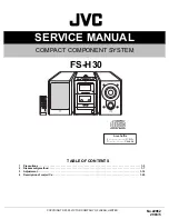
SERVICE MANUAL
COPYRIGHT © 2003 VICTOR COMPANY OF JAPAN, LIMITED
No.22062
2003/5
COMPACT
COMPONENT SYSTEM
22062
2003
5
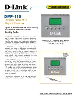
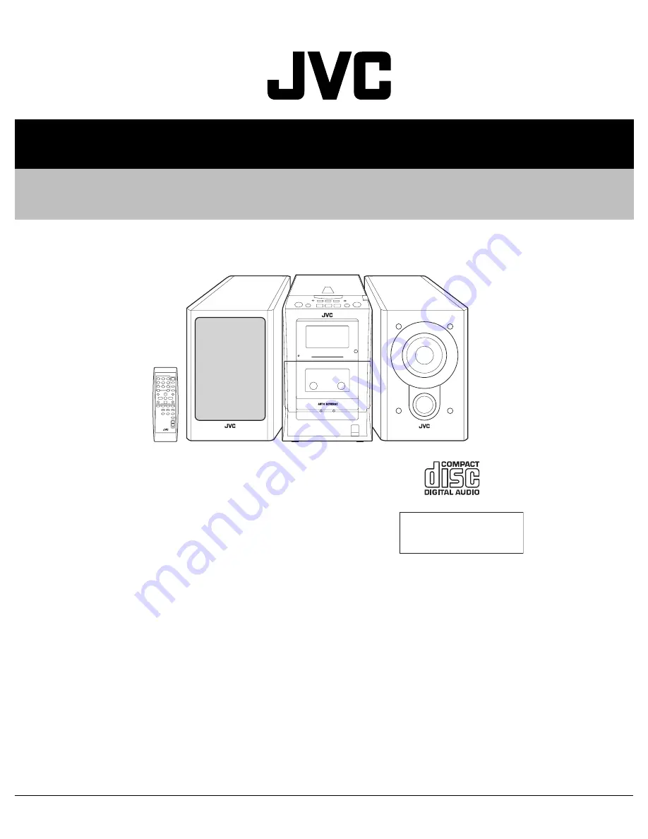
FS-H30
TABLE OF CONTENTS
1
Precautions . . . . . . . . . . . . . . . . . . . . . . . . . . . . . . . . . . . . . . . . . . . . . . . . . . . . . . . . . . . . . . . . . . . . . . . . . . 1-3
2
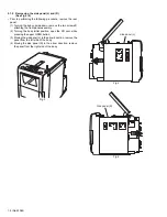
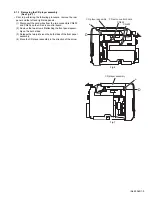
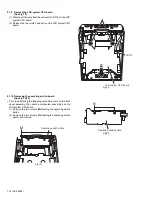
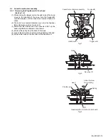
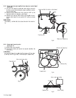
Disassembly method . . . . . . . . . . . . . . . . . . . . . . . . . . . . . . . . . . . . . . . . . . . . . . . . . . . . . . . . . . . . . . . . . . 1-7
3
Adjustment. . . . . . . . . . . . . . . . . . . . . . . . . . . . . . . . . . . . . . . . . . . . . . . . . . . . . . . . . . . . . . . . . . . . . . . . . . 1-19
4
Description of major ICs . . . . . . . . . . . . . . . . . . . . . . . . . . . . . . . . . . . . . . . . . . . . . . . . . . . . . . . . . . . . . . . 1-25
COMPACT COMPONENT SYSTEM
Area Suffix
J -------------------- U.S.A.
C ------------------ Canada